LMK1D1212
Overview
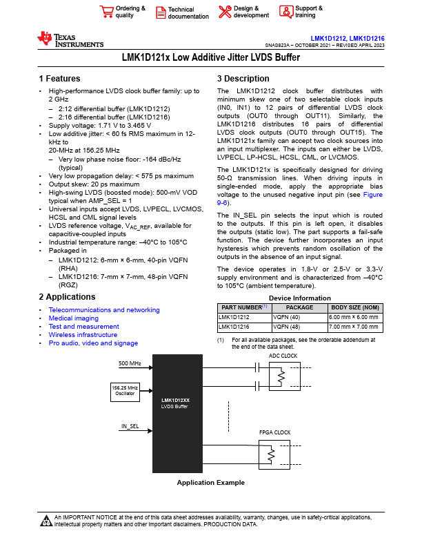
The LMK1D1212 clock buffer distributes with minimum skew one of two selectable clock inputs (IN0, IN1) to 12 pairs of differential LVDS clock outputs (OUT0 through OUT11). Similarly, the LMK1D1216 distributes 16 pairs of differential LVDS clock outputs (OUT0 through OUT15).
- High-performance LVDS clock buffer family: up to 2 GHz - 2:12 differential buffer (LMK1D1212) - 2:16 differential buffer (LMK1D1216)
- Supply voltage: 1.71 V to 3.465 V
- Low additive jitter: < 60 fs RMS maximum in 12- kHz to 20-MHz at 156.25 MHz - Very low phase noise floor: -164 dBc/Hz (typical)
- Very low propagation delay: < 575 ps maximum
- Output skew: 20 ps maximum
- High-swing LVDS (boosted mode): 500-mV VOD typical when AMP_SEL = 1
- Universal inputs accept LVDS, LVPECL, LVCMOS, HCSL and CML signal levels
- LVDS reference voltage, VAC_REF, available for capacitive-coupled inputs
- Industrial temperature range: -40°C to 105°C
- Packaged in - LMK1D1212: 6-mm × 6-mm, 40-pin VQFN (RHA) - LMK1D1216: 7-mm × 7-mm, 48-pin VQFN (RGZ)