Datasheet4U Logo Datasheet4U.com

LVC00A - Quadruple 2-Input Positive-NAND Gate

General Description

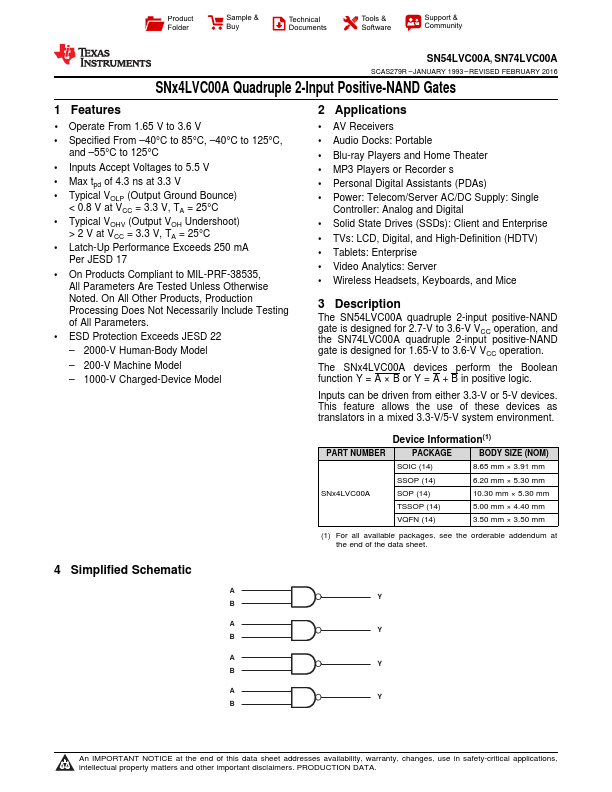
The SN54LVC00A quadruple 2-input positive-NAND gate is designed for 2.7-V to 3.6-V VCC operation, and the SN74LVC00A quadruple 2-input positive-NAND gate is designed for 1.65-V to 3.6-V VCC operation.

The SNx4LVC00A devices perform the Boolean function Y = A × B or Y = A + B in positive logic.

Key Features

  • 1 Operate From 1.65 V to 3.6 V.
  • Specified From.
  • 40°C to 85°C,.
  • 40°C to 125°C, and.
  • 55°C to 125°C.
  • Inputs Accept Voltages to 5.5 V.
  • Max tpd of 4.3 ns at 3.3 V.
  • Typical VOLP (Output Ground Bounce) < 0.8 V at VCC = 3.3 V, TA = 25°C.
  • Typical VOHV (Output VOH Undershoot) > 2 V at VCC = 3.3 V, TA = 25°C.
  • Latch-Up Performance Exceeds 250 mA Per JESD 17.
  • On Products Compliant to MIL-PRF-38535, All Parameters.

📥 Download Datasheet

Full PDF Text Transcription (Reference)

The following content is an automatically extracted verbatim text from the original manufacturer datasheet and is provided for reference purposes only.

View original datasheet text
Product Folder Sample & Buy Technical Documents Tools & Software Support & Community SN54LVC00A, SN74LVC00A SCAS279R – JANUARY 1993 – REVISED FEBRUARY 2016 SNx4LVC00A Quadruple 2-Input Positive-NAND Gates 1 Features •1 Operate From 1.65 V to 3.6 V • Specified From –40°C to 85°C, –40°C to 125°C, and –55°C to 125°C • Inputs Accept Voltages to 5.5 V • Max tpd of 4.3 ns at 3.3 V • Typical VOLP (Output Ground Bounce) < 0.8 V at VCC = 3.3 V, TA = 25°C • Typical VOHV (Output VOH Undershoot) > 2 V at VCC = 3.3 V, TA = 25°C • Latch-Up Performance Exceeds 250 mA Per JESD 17 • On Products Compliant to MIL-PRF-38535, All Parameters Are Tested Unless Otherwise Noted. On All Other Products, Production Processing Does Not Necessarily Include Testing of All Parameters.