SN54ABTH16245 Overview
Key Specifications
Output Type (varies by manufacturer): TTL
Description
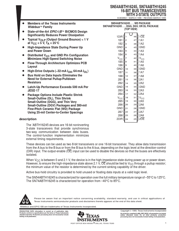
SN54ABTH16245, SN74ABTH16245 16-BIT BUS TRANSCEIVERS WITH 3-STATE OUTPUTS SCBS662I – MARCH 1996 – REVISED MARCH 1999 SN54ABTH16245. WD PACKAGE SN74ABTH16245.