Texas Instruments SN54ALS299
The SN54ALS299 is characterized for operation over the full military temperature range of – 55°C to 125°C. The SN74ALS299 is characterized for operation from 0°C to 70°C.SN54ALS299 Specifications
- Output Type : TTL
Source:
Octopart
| Part No. | SN54ALS299 |
|---|---|
| Datasheet | SN54ALS299 Download |
| Manufacturer |  Texas Instruments |
| Description | 8-BIT UNIVERSAL SHIFT/STORAGE REGISTER |
| Buy | Stock & Price |
APPLICATIONS
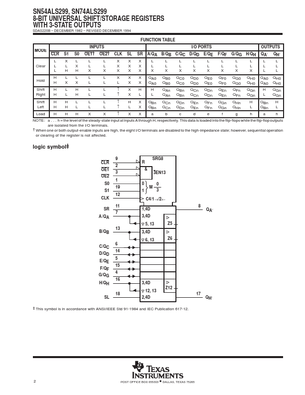
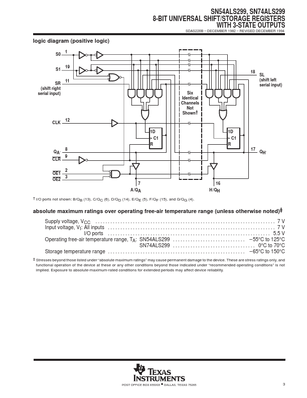
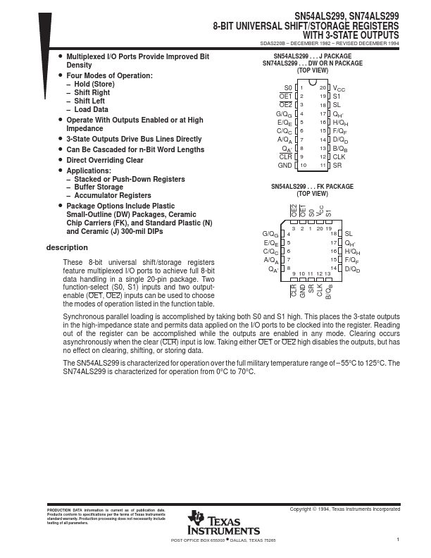
: – Stacked or Push-Down Registers – Buffer Storage – Accumulator Registers● Package Options Include Plastic Small-Outline (DW) Packages, Ceramic Chip Carriers (FK), and Standard Plastic (N) and Ceramic (J) 300-mil DIPs description These 8-bit universal shift /storage registers feature multiplexed I/O ports to achieve full 8-bit data handling in a single 20-pin package. Two function-select (S0, S1) inputs and two outputenable (OE1, OE2) inputs can be used to choose the modes of operation listed in the function table. CLR GND SR CLK B/QB SN54ALS299 . . . J PACKAGE SN74ALS299 . . . DW OR N PACKAGE (TOP VIEW) S0 1 OE1 2 OE2 3 G/QG 4 E/QE 5 C/QC 6 A/QA 7 QA′ 8 CLR 9 GND 10 20 VCC 19 S1 18 SL 17 QH′ 16 H/QH 15 F/QF 14 D/QD 13 B/QB 12 CLK 11 SR SN54ALS299 . . . FK PACKAGE (TOP VIEW) OE2 OE1 S0 VCC S1 G/QG E/QE C/QC A/QA QA′ 3 2 1 20 19 4 18 5 17 6 16 7 15 8 14 9 10 11 12 13 SL QH′ H/QH F/QF D/QD Synchronous parallel loading is accomplished by taking both S0 and S1 high. This places the 3-state outputs in the high-impedance state and permits data applied on the I/O ports to be clocked into the register.