SN54LS374
SN54LS374 is OCTAL D-TYPE TRANSPARENT LATCHES AND EDGE-TRIGGERED FLIP-FLOPS manufactured by Texas Instruments.
- Part of the SN54LS373 comparator family.
- Part of the SN54LS373 comparator family.
description
These 8-bit registers feature
3-state outputs designed specifically for driving highly capacitive or relatively low-impedance loads. The high-impedance 3-state and increased high-logic-level drive provide these registers with the capability of being connected directly to and driving the bus lines in a bus-organized system without need for interface or pullup ponents. These devices are particularly attractive for implementing buffer registers, I/O ports, bidirectional bus drivers, and working registers.
The eight latches of the ’LS373 and ’S373 are transparent D-type latches, meaning that while the enable (C or CLK) input is high, the Q outputs follow the data (D) inputs. When C or CLK is taken low, the output is latched at the level of the data that was set up.
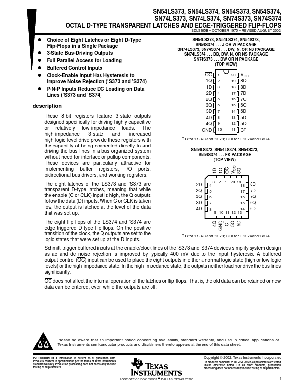
SN54LS373, SN54LS374, SN54S373, SN54S374 . . . J OR W PACKAGE
SN74LS373, SN74S374 . . . DW, N, OR NS PACKAGE SN74LS374 . . . DB, DW, N, OR NS PACKAGE SN74S373 . . . DW OR N PACKAGE (TOP VIEW)
OC 1Q 1D 2D 2Q 3Q 3D 4D 4Q GND
1 2 3 4 5 6 7 8 9 10
20 VCC 19 8Q 18 8D 17 7D 16 7Q 15 6Q 14 6D 13 5D 12 5Q 11 C†
† C for ’LS373 and ’S373; CLK for ’LS374 and ’S374.
SN54LS373, SN54LS374, SN54S373, SN54S374 . . . FK PACKAGE (TOP VIEW)
2D
3 2 1 20 19 4 18
8D
2Q 5
17 7D
3Q 6
16 7Q
3D 7
15 6Q
4D 8
14 6D
9 10 11 12 13
4Q 1D GND 1Q
C† OC 5Q VCC 5D 8Q
The eight flip-flops of the ’LS374 and ’S374 are edge-triggered D-type flip-flops. On the positive transition of the clock, the Q outputs are set to the logic states that were set up at the D inputs.
† C for ’LS373 and ’S373; CLK for ’LS374 and ’S374.
Schmitt-trigger buffered inputs at the enable/clock lines of the ’S373 and ’S374 devices simplify system design as ac and dc noise rejection is improved by typically 400 m V due to the input hysteresis. A buffered output-control (OC) input can be used to place the eight outputs in either a normal logic state (high or low logic levels) or the high-impedance state. In the high-impedance state, the...