Datasheet4U Logo Datasheet4U.com

SN54LVC00A - Quadruple 2-Input Positive-NAND Gate

General Description

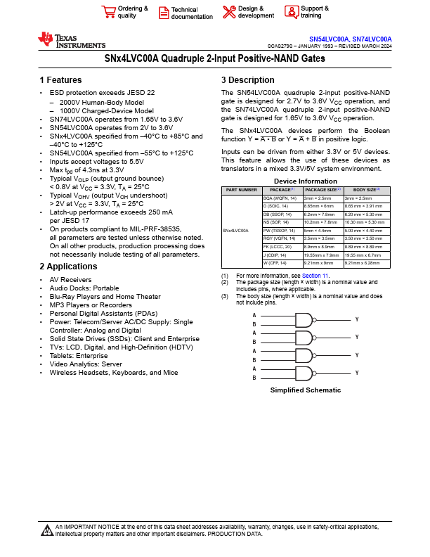
The SN54LVC00A quadruple 2-input positive-NAND gate is designed for 2.7V to 3.6V VCC operation, and the SN74LVC00A quadruple 2-input positive-NAND gate is designed for 1.65V to 3.6V VCC operation.

B or Y = A + B in positive logic.

Key Features

  • ESD protection exceeds JESD 22.
  • 2000V Human-Body Model.
  • 1000V Charged-Device Model.
  • SN74LVC00A operates from 1.65V to 3.6V.
  • SN54LVC00A operates from 2V to 3.6V.
  • SNx4LVC00A specified from.
  • 40°C to +85°C and.
  • 40°C to +125°C.
  • SN54LVC00A specified from.
  • 55°C to +125°C.
  • Inputs accept voltages to 5.5V.
  • Max tpd of 4.3ns at 3.3V.
  • Typical VOLP (output ground bounce) < 0.8V at VCC = 3.3V, TA.

📥 Download Datasheet

Full PDF Text Transcription (Reference)

The following content is an automatically extracted verbatim text from the original manufacturer datasheet and is provided for reference purposes only.

View original datasheet text
SN54LVC00A, SN74LVC00A SCAS279S – JANUARY 1993 – REVISED MARCH 2024 SNx4LVC00A Quadruple 2-Input Positive-NAND Gates 1 Features • ESD protection exceeds JESD 22 – 2000V Human-Body Model – 1000V Charged-Device Model • SN74LVC00A operates from 1.65V to 3.6V • SN54LVC00A operates from 2V to 3.6V • SNx4LVC00A specified from –40°C to +85°C and –40°C to +125°C • SN54LVC00A specified from –55°C to +125°C • Inputs accept voltages to 5.5V • Max tpd of 4.3ns at 3.3V • Typical VOLP (output ground bounce) < 0.8V at VCC = 3.3V, TA = 25°C • Typical VOHV (output VOH undershoot) > 2V at VCC = 3.3V, TA = 25°C • Latch-up performance exceeds 250 mA per JESD 17 • On products compliant to MIL-PRF-38535, all parameters are tested unless otherwise noted.