SN64BCT25244 Overview
Key Specifications
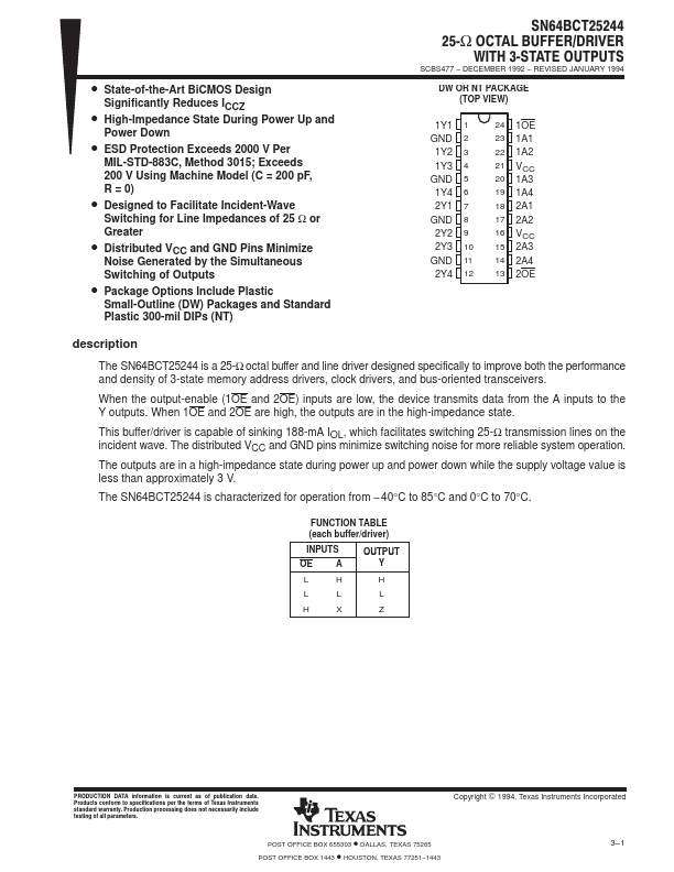
Package: SOIC
Mount Type: Surface Mount
Pins: 24
Operating Voltage: 5 V
Description
The SN64BCT25244 is a 25-Ω octal buffer and line driver designed specifically to improve both the performance and density of 3-state memory address drivers, clock drivers, and bus-oriented transceivers. When the output-enable (1OE and 2OE) inputs are low, the device transmits data from the A inputs to the Y outputs.