• Part: SN65CML100
  • Description: 1.5-Gbps LVDS/LVPECL/CML-TO-CML TRANSLATOR/REPEATER
  • Manufacturer: Texas Instruments
  • Size: 1.38 MB
Download SN65CML100 Datasheet PDF
Texas Instruments
SN65CML100
SN65CML100 is 1.5-Gbps LVDS/LVPECL/CML-TO-CML TRANSLATOR/REPEATER manufactured by Texas Instruments.
FEATURES - Provides Level Translation From LVDS or LVPECL to CML, Repeating From CML to CML - Signaling Rates(1) up to 1.5 Gbps - CML patible Output Directly Drives Devices With 3.3-V, 2.5-V, or 1.8-V Supplies - Total Jitter < 70 ps - Low 100 ps (Max) Part-To-Part Skew - Wide mon-Mode Receiver Capability Allows Direct Coupling of Input Signals - 25 m V of Receiver Input Threshold Hysteresis Over 0-V to 4-V mon-Mode Range - Propagation Delay Times, 800 ps Maximum - 3.3-V Supply Operation - Available in SOIC and MSOP Packages APPLICATIONS - Level Translation - 622-MHz Central Office Clock Distribution - High-Speed Network Routing - Wireless Basestations - Low Jitter Clock Repeater(1) (1) The signaling rate of a line is the number of voltage transitions that are made per second expressed in the units bps (bits per second). FUNCTIONAL DIAGRAM DESCRIPTION 
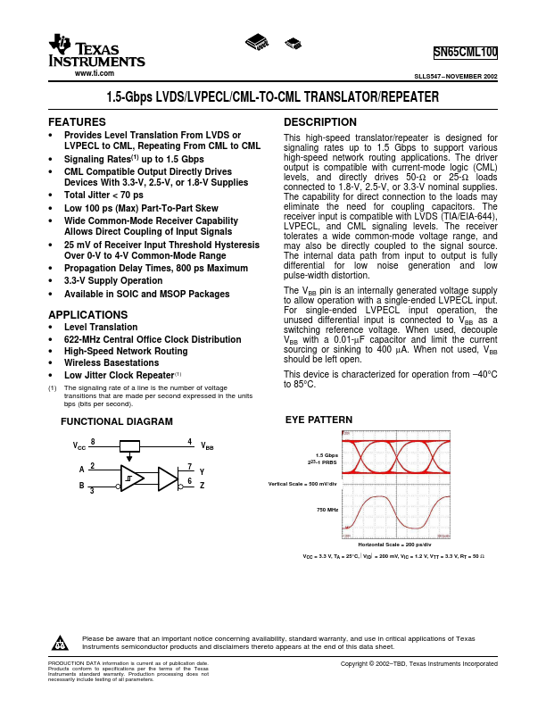
This high-speed translator/repeater is designed for signaling rates up to 1.5 Gbps to support various high-speed network routing applications. The driver output is patible with current-mode logic (CML) levels, and directly drives 50-Ω or 25-Ω loads connected to 1.8-V, 2.5-V, or 3.3-V nominal supplies. The capability for direct connection to the loads may eliminate the need for coupling capacitors. The receiver input is patible with LVDS (TIA/EIA-644), LVPECL, and CML signaling levels. The receiver tolerates a wide mon-mode voltage range, and may also be directly coupled to the signal source. The internal data path from input to output is fully differential for low noise generation and low pulse-width distortion. The VBB pin is an internally generated voltage supply to allow operation with a single-ended LVPECL input. For single-ended LVPECL input operation, the unused differential input is connected to VBB as a switching reference voltage. When used, decouple VBB with a 0.01-µF capacitor and limit the current sourcing or sinking to 400 µA. When not used, VBB should be left open. This device is characterized for...