SN65LVDM22
SN65LVDM22 is DUAL MULTIPLEXED LVDS REPEATERS manufactured by Texas Instruments.
- Part of the SN65LVDS22 comparator family.
- Part of the SN65LVDS22 comparator family.
FEATURES
- Meets or Exceeds the Requirements of ANSI TIA/EIA-644-1995 Standard
- Designed for Clock Rates up to 200 MHz (400 Mbps)
- Designed for Data Rates up to 250 Mbps
- Pin patible With SN65LVDS122 and
SN65LVDT122, 1.5 Gbps 2x2 Crosspoint Switch From TI
- ESD Protection Exceeds 12 k V on Bus Pins
- Operates From a Single 3.3-V Supply
- Low-Voltage Differential Signaling With
Output Voltages of 350 m V Into:
- 100-Ω Load (SN65LVDS22)
- 50-Ω Load (SN65LVDM22)
- Propagation Delay Time; 4 ns Typ
- Power Dissipation at 400 Mbps of 150 m W
- Bus Pins Are High Impedance When Disabled or With VCC Less Than 1.5 V
- LVTTL Levels Are 5 V Tolerant
- Open-Circuit Fail Safe Receiver
DESCRIPTION
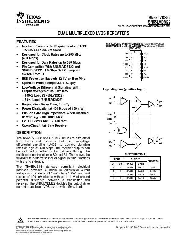
The SN65LVDS22 and SN65LVDM22 are differential line drivers and receivers that use low-voltage differential signaling (LVDS) to achieve signaling rates as high as 400 Mbps. The receiver outputs can be switched to either or both drivers through the multiplexer control signals S0 and S1. This allows the flexibility to perform splitter or signal routing functions with a single device.
The TIA/EIA-644 standard pliant electrical interface provides a minimum differential output voltage magnitude of 247 m V into a 100-Ω load and receipt of 100 m V signals with up to 1 V of ground potential difference between a transmitter and receiver. The SN65LVDM22 doubles the output drive current to achieve LVDS levels with a 50-Ω load.
SN65LVDS22D and SN65LVDS22PW (Marked as LVDS22) SN65LVDM22D and SN65LVDM22PW (Marked as LVDM22)
(TOP VIEW)
1B 1 1A 2 S0 3 1DE 4 S1 5 2A 6 2B 7 GND 8
16 VCC 15 VCC 14 1Y 13 1Z 12 2DE 11 2Z 10 2Y 9 GND logic diagram (positive logic)
2 1A
+
1B 1
_
4 1DE
12 2DE
3 S0
14 1Y
13 1Z
5 S1
6 2A
+
7...