SN65LVDS311
FEATURES
- 2.8 × 2.8mm package size
- 1.8V input signal swing
- 24-Bit RGB Data, 3 Control Bits, 1 Parity Bit and 2 Reserved Bits Transmitted over 1, 2 or 3 Differential Lines
- Sub LVDS Differential Voltage Levels
- Three Operating Modes to Conserve Power
- Active-Mode QVGA 17.4m W (typ)
- Active-Mode VGA 28.8m W (typ)
- Shutdown Mode ≈ 0.5μA (typ)
- Standby Mode ≈ 0.5μA (typ)
- ESD Rating > 3k V (HBM)
- Pixel Clock Range of 4MHz- 65MHz
- Failsafe on all CMOS Inputs
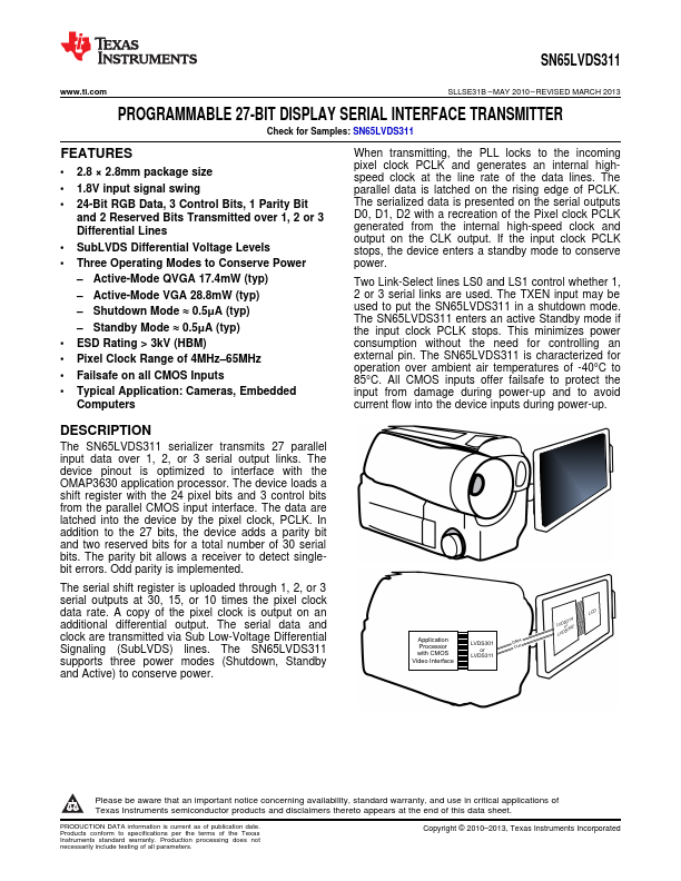
- Typical Application: Cameras, Embedded puters
When transmitting, the PLL locks to the ining pixel clock PCLK and generates an internal highspeed clock at the line rate of the data lines. The parallel data is latched on the rising edge of PCLK. The serialized data is presented on the serial outputs D0, D1, D2 with a recreation of the Pixel clock PCLK generated from the internal high-speed clock and output on the CLK output. If the input clock PCLK stops, the device enters a standby mode to conserve power.
Two Link-Select...