SN7489 Datasheet Text
SN7489 64-BIT RANDOM-ACCESS READ/WRITE MEMORY
- For Application as a"Scratch Pad" Memory with Nondestructive Read-Out
- Fully Decoded Memory Organized as 16 Words of Four Bits Each
- Fast Access Time . . . 3 3 ns Typical
- Diode-Clamped, Buffered Inputs
- Open-Collector Outputs Provide Wire-AND Capability
- Typical Power Dissipation . . . 3 7 5 mW
- patible with Most TTL Circuits description
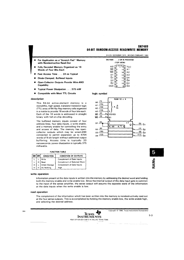
This 64-bit active-element memory is a monolithic, high-speed, transistor-transistor logic (TTL) array of 64 flip-flop memory cells organized in a matrix to provide 16 words of four bits each. Each of the 16 words is addressed in straight binary with full on-chip decoding.
The buffered memory inputs consist of four address lines, four data inputs, a write enable, and a memory enable for controlling the entry and access of data. The memory has opencollector outputs which may be wired-AND connected to permit expansion up to 4704 words of N-bit length without additional output buffering. Access time is typically 33 nanoseconds; power dissipation is typically 375 milliwatts.
D1416, DECEMBER 1972-REV1SED FEBRUARY 1984
SN7489 . J OR N PACKAGE (TOP VIEWI
AO C . ME C 2 WE C 3 01 C 4 Q1 : 5 D2 C 6
Q2 C 7 GND C 8
U , 6 H VCC 15 3 A 1 14 D A 2 13 J A 3 12 U D 4 11 3 Q 4 10 H D 3 9 ] Q3 logic symbol
AO 111 A1 (15| A2 (14) A3 (13) me^L T77F (31 -Cs,
RAM 1 6 X 4
(4)
- 2
- (61 0 3
- (101 D4
- (12)
1
A, 2D
>1 ^ ^
A, 1. 3 |
~
^
^
^...