SN74AHCT1G125 Overview
Description
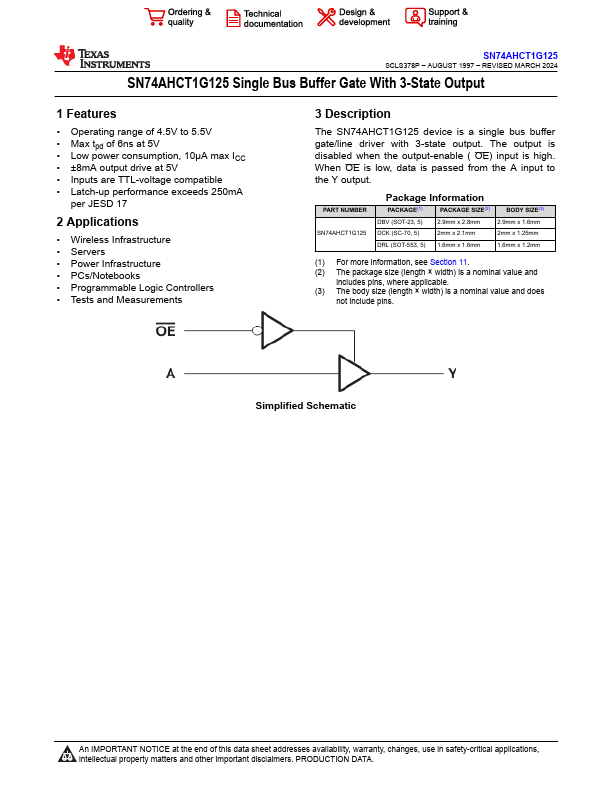
The SN74AHCT1G125 device is a single bus buffer gate/line driver with 3-state output. The output is disabled when the output-enable ( OE) input is high.
Key Features
- Operating range of 4.5V to 5.5V
- Max tpd of 6ns at 5V
- Low power consumption, 10µA max ICC
- ±8mA output drive at 5V
- Inputs are TTL-voltage compatible
- Latch-up performance exceeds 250mA per JESD 17