SN74ALVC00 Overview
Key Specifications
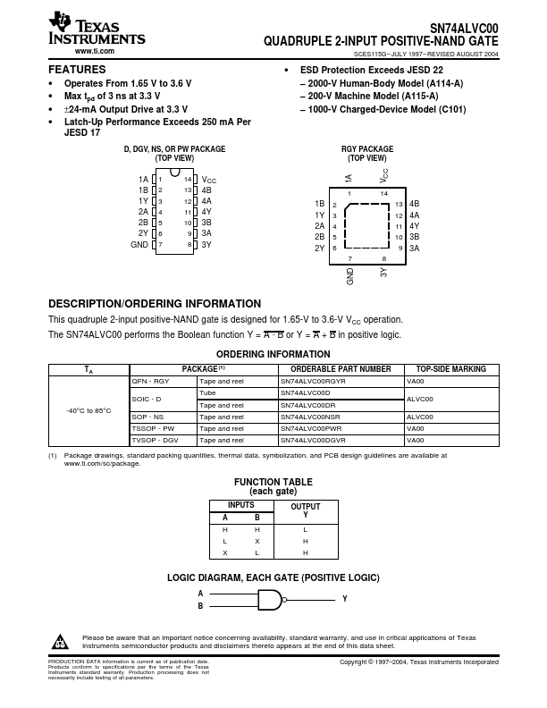
Package: SOP
Mount Type: Surface Mount
Pins: 14
Max Voltage (typical range): 3.6 V
Key Features
- Operates From 1.65 V to 3.6 V
- Max tpd of 3 ns at 3.3 V
- ±24-mA Output Drive at 3.3 V
| Part | SN74ALVC00 |
|---|---|
| Description | QUADRUPLE 2-INPUT POSITIVE-NAND GATE |
| Manufacturer | Texas Instruments |
| Size | 621.91 KB |
Package: SOP
Mount Type: Surface Mount
Pins: 14
Max Voltage (typical range): 3.6 V
| Seller | Inventory | Price Breaks | Buy |
|---|---|---|---|
| Rochester Electronics | 94000 | 100+ : 0.2682 USD 500+ : 0.2414 USD 1000+ : 0.2226 USD 10000+ : 0.1985 USD |
View Offer |
| DigiKey | 1925 | 1+ : 0.52 USD 10+ : 0.362 USD 25+ : 0.324 USD 100+ : 0.2817 USD |
View Offer |
| Part Number | Manufacturer | Description |
|---|---|---|
| NSi6602 | NOVOSENSE | High Reliability Isolated Dual-Channel Gate Driver |
| NSi6801 | NOVOSENSE | Single-Channel Isolated Gate Driver |
| FD2103 | Fortior | 180V Half-Bridge Gate Driver |