SN74AUP1G07 Overview
Key Specifications
Package: SOT-23
Mount Type: Surface Mount
Pins: 5
Max Voltage (typical range): 3.6 V
Description
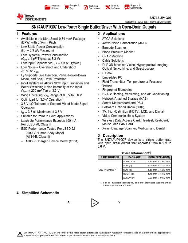
The SN74AUP1G07 device is a single buffer gate with open drain output that operates from 0.8 V to 3.6 V. Device Information(1) PART NUMB.
Key Features
- 1 Available in the Ultra Small 0.64 mm2 Package (DPW) with 0.5-mm Pitch
- Low Static-Power Consumption (ICC = 0.9 µA Maximum)
- Low Dynamic-Power Consumption (Cpd = 1 pF Typical at 3.3 V)
- Low Input Capacitance (Ci = 1.5 pF Typical)
- Low Noise – Overshoot and Undershoot <10% of VCC