Datasheet4U Logo Datasheet4U.com

SN74AUP1T08 - Positive-AND Gate

General Description

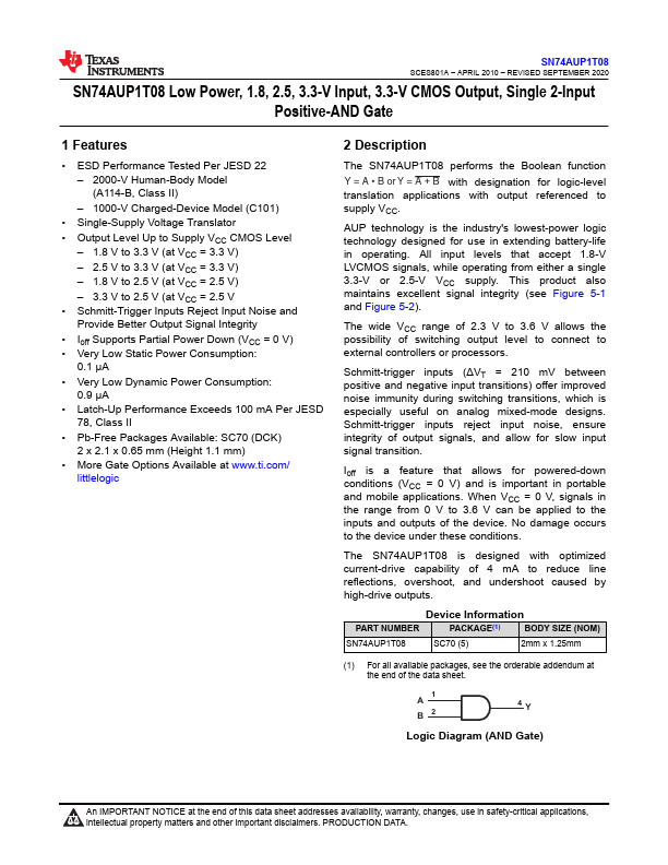
The SN74AUP1T08 performs the Boolean function Y = A

B or Y = A + B with designation for logic-level translation applications with output referenced to supply VCC.

AUP technology is the industry's lowest-power logic technology designed for use in extending battery-life in operating.

Key Features

  • ESD Performance Tested Per JESD 22.
  • 2000-V Human-Body Model (A114-B, Class II).
  • 1000-V Charged-Device Model (C101).
  • Single-Supply Voltage Translator.
  • Output Level Up to Supply VCC CMOS Level.
  • 1.8 V to 3.3 V (at VCC = 3.3 V).
  • 2.5 V to 3.3 V (at VCC = 3.3 V).
  • 1.8 V to 2.5 V (at VCC = 2.5 V).
  • 3.3 V to 2.5 V (at VCC = 2.5 V.
  • Schmitt-Trigger Inputs Reject Input Noise and Provide Better Output Signal Integrity.

📥 Download Datasheet

Full PDF Text Transcription (Reference)

The following content is an automatically extracted verbatim text from the original manufacturer datasheet and is provided for reference purposes only.

View original datasheet text
www.ti.com SN74AUP1T08 SCES801A – APRIL 2010 – REVISEDSSENP7T4EAMUBEPR12T00280 SCES801A – APRIL 2010 – REVISED SEPTEMBER 2020 SN74AUP1T08 Low Power, 1.8, 2.5, 3.3-V Input, 3.3-V CMOS Output, Single 2-Input Positive-AND Gate 1 Features • ESD Performance Tested Per JESD 22 – 2000-V Human-Body Model (A114-B, Class II) – 1000-V Charged-Device Model (C101) • Single-Supply Voltage Translator • Output Level Up to Supply VCC CMOS Level – 1.8 V to 3.3 V (at VCC = 3.3 V) – 2.5 V to 3.3 V (at VCC = 3.3 V) – 1.8 V to 2.5 V (at VCC = 2.5 V) – 3.3 V to 2.5 V (at VCC = 2.5 V • Schmitt-Trigger Inputs Reject Input Noise and Provide Better Output Signal Integrity • Ioff Supports Partial Power Down (VCC = 0 V) • Very Low Static Power Consumption: 0.1 µA • Very Low Dynamic Power Consumption: 0.