SN74AUP1T32 Overview
Key Specifications
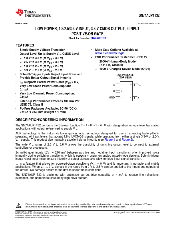
Package: SC
Mount Type: Surface Mount
Pins: 5
Max Voltage (typical range): 3.6 V
Key Features
- Single-Supply Voltage Translator
- Schmitt-Trigger Inputs Reject Input Noise and Provide Better Output Signal Integrity
- Ioff Supports Partial Power Down (VCC = 0 V)
- Very Low Static Power Consumption: 0.1 µA
- Very Low Dynamic Power Consumption: 0.9 µA