SN74AUP2G07 Overview
Key Specifications
Mount Type: Surface Mount
Pins: 6
Max Voltage (typical range): 3.6 V
Min Voltage (typical range): 800 mV
Description
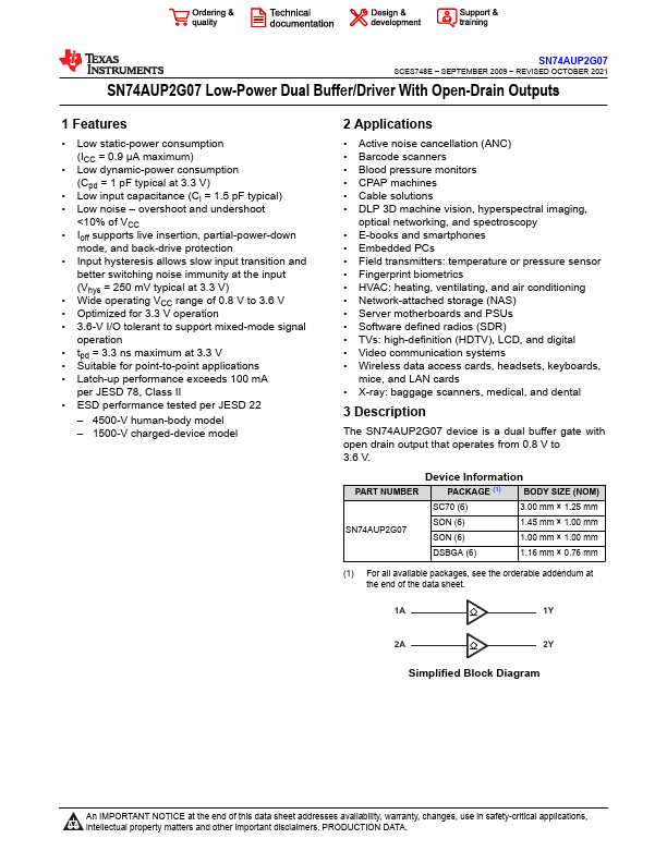
The SN74AUP2G07 device is a dual buffer gate with open drain output that operates from 0.8 V to 3.6 V. Device Information PART NUMBER PACKAGE (1) BODY SIZE (NOM) SC70 (6) 3.00 mm × 1.25 mm SN74AUP2G07 SON (6) SON (6) 1.45 mm × 1.00 mm 1.00 mm × 1.00 mm DSBGA (6) 1.16 mm × 0.76 mm (1) For.
Key Features
- Low static-power consumption (ICC = 0.9 µA maximum)
- Low dynamic-power consumption (Cpd = 1 pF typical at 3.3 V)
- Low input capacitance (Ci = 1.5 pF typical)
- Low noise – overshoot and undershoot <10% of VCC
- Ioff supports live insertion, partial-power-down mode, and back-drive protection