SN74CB3Q3125 Overview
Key Specifications
Package: TFSOP
Mount Type: Surface Mount
Pins: 14
Max Voltage (typical range): 3.6 V
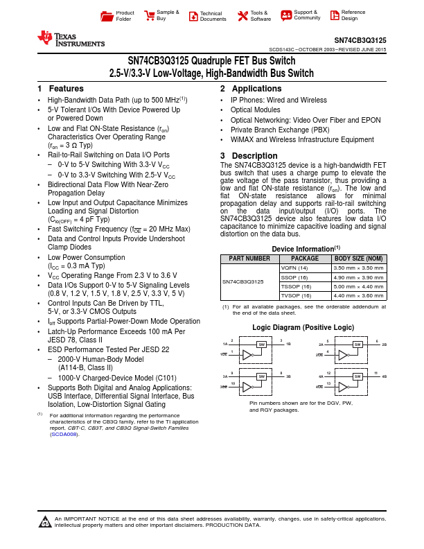
Description
The SN74CB3Q3125 device is a high-bandwidth FET bus switch that uses a charge pump to elev.
Key Features
- 1 High-Bandwidth Data Path (up to 500 MHz(1))
- 5-V Tolerant I/Os With Device Powered Up or Powered Down
- Low and Flat ON-State Resistance (ron) Characteristics Over Operating Range (ron = 3 Ω Typ)
- Rail-to-Rail Switching on Data I/O Ports – 0-V to 5-V Switching With 3.3-V VCC – 0-V to 3.3-V Switching With 2.5-V VCC
- Bidirectional Data Flow With Near-Zero Propagation Delay