SN74LV1T125 Overview
Key Specifications
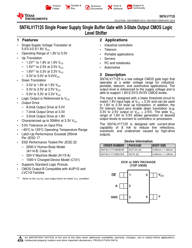
Package: SC
Mount Type: Surface Mount
Pins: 5
Max Voltage (typical range): 5.5 V
Description
SN74LV1T125 is a low voltage CMOS gate logic that operates at a wider voltage range for industrial, portable, telecom, and automotive applications. The output level is referenced to the supply voltage and is able to support 1.8V/2.5V/3.3V/5V CMOS levels.
Key Features
- Operating Range of 1.8V to 5.5V
- Up Translation – 1.2V(1) to 1.8V at 1.8V VCC – 1.5V(1) to 2.5V at 2.5V VCC – 1.8V(1) to 3.3V at 3.3V VCC – 3.3V to 5.0V at 5.0VVCC
- Down Translation – 3.3V to 1.8V at 1.8V VCC – 3.3V to 2.5V at 2.5V VCC – 5.0V to 3.3V at 3.3V VCC
- Logic Output is Referenced to VCC
- Output Drive – 8.0mA Output Drive at 5.0V – 7.0mA Output Drive at 3.3V – 3.0mA Output Drive at 1.8V