SN74LV541AT Overview
Key Specifications
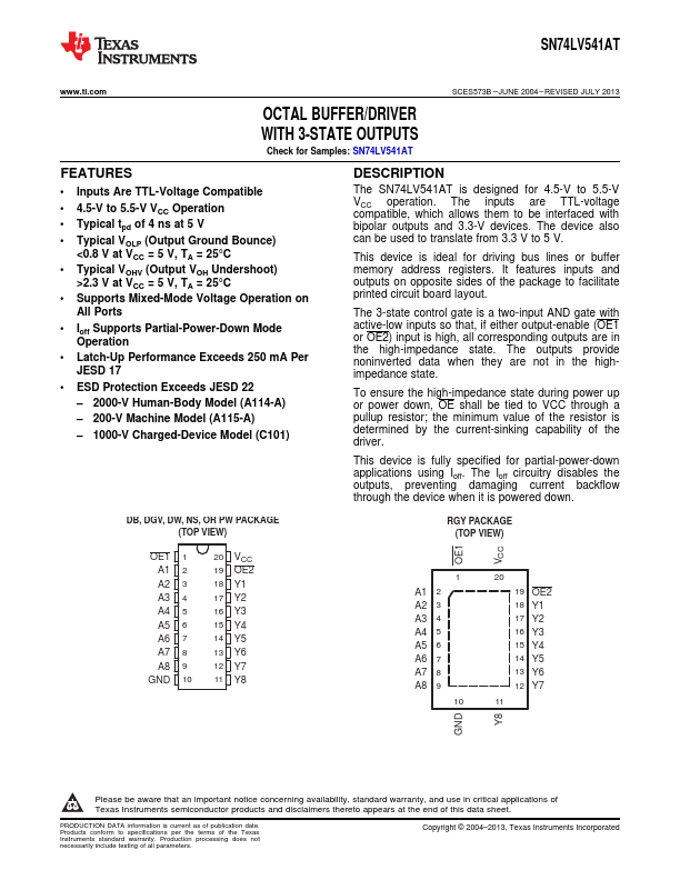
Package: TFSOP
Mount Type: Surface Mount
Pins: 20
Operating Voltage: 5 V
Description
The SN74LV541AT is designed for 4.5-V to 5.5-V VCC operation. The inputs are TTL-voltage compatible, which allows them to be interfaced with bipolar outputs and 3.3-V devices.
Key Features
- Inputs Are TTL-Voltage Compatible
- 4.5-V to 5.5-V VCC Operation
- Typical tpd of 4 ns at 5 V
- Typical VOLP (Output Ground Bounce) <0.8 V at VCC = 5 V, TA = 25°C
- Typical VOHV (Output VOH Undershoot) >2.3 V at VCC = 5 V, TA = 25°C