Datasheet4U Logo Datasheet4U.com

SN74LVC126A-Q1 - Automotive Quadruple Bus Buffer Gate

General Description

This quadruple bus buffer gate is designed for 1.65V to 3.6V VCC operation.

Key Features

  • Qualified for automotive.

📥 Download Datasheet

Full PDF Text Transcription (Reference)

The following content is an automatically extracted verbatim text from the original manufacturer datasheet and is provided for reference purposes only.

View original datasheet text
SN74LVC126A-Q1 SCAS763C – FEBRUARY 2004 – REVISED MAY 2024 SN74LVC126A-Q1 Automotive Quadruple Bus Buffer Gate With 3-State Outputs 1 Features • Qualified for automotive applications • Operates from 1.65V to 3.6V • Inputs accept voltages to 5.5V • Max tpd of 4.7ns at 3.3V • Typical VOLP (output ground bounce) <0.8V at VCC = 3.3V, TA = 25°C • Typical VOHV (output VOH undershoot) >2V at VCC = 3.3V, TA = 25°C • Latch-up performance exceeds 250mA per JESD 17 • ESD protection exceeds JESD 22 1 1OE 2 1A 3 1Y 2 Description 
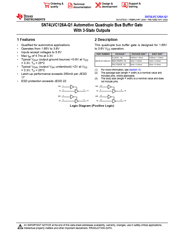
This quadruple bus buffer gate is designed for 1.65V to 3.6V VCC operation. PART NUMBER PACKAGE(1) D (SOIC, 14) SN74LVC126A-Q1 BQA (WQFN, 14) PW (TSSOP, 14) PACKAGE SIZE(2) 8.65mm × 6mm 3mm × 2.5mm 5mm × 6.4mm BODY SIZE(3) 8.65mm × 3.9mm 3mm × 2.5mm 5mm × 4.