Datasheet4U Logo Datasheet4U.com

SN74LVC2G125-Q1 - Dual Bus Buffer Gate

General Description

The SN74LVC2G125-Q1 is a dual bus buffer gate designed for 1.65-V to 5.5-V VCC operation.

Key Features

  • 1.
  • Qualified for Automotive.

📥 Download Datasheet

Full PDF Text Transcription (Reference)

The following content is an automatically extracted verbatim text from the original manufacturer datasheet and is provided for reference purposes only.

View original datasheet text
SN74LVC2G125-Q1 www.ti.com DUAL BUS BUFFER GATE WITH 3-STATE OUTPUTS Check for Samples: SN74LVC2G125-Q1 SCES559C – MARCH 2004 – REVISED MARCH 2011 FEATURES 1 • Qualified for Automotive Applications • Supports 5-V VCC Operation • Inputs Accept Voltages to 5.5 V • Max tpd of 4.3 ns at 3.3 V • Low Power Consumption, 10-μA Max ICC • ±24-mA Output Drive at 3.3 V • Typical VOLP (Output Ground Bounce) <0.8 V at VCC = 3.3 V, TA = 25°C • Typical VOHV (Output VOH Undershoot) >2 V at VCC = 3.3 V, TA = 25°C • Ioff Supports Partial-Power-Down Mode Operation • 
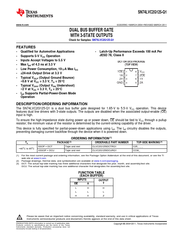
Latch-Up Performance Exceeds 100 mA Per JESD 78, Class II DCT OR DCU PACKAGE (TOP VIEW) 1OE 1A 2Y GND 1 2 3 4 8 VCC 7 2OE 6 1Y 5 2A DESCRIPTION/ORDERING INFORMATION The SN74LVC2G125-Q1 is a dual bus buffer gate designed for 1.65-V to 5.