SN74LVC2G34
Features
- 1 Available in the Texas Instruments Nano Free™ Package
- Supports 5.5-V VCC Operation
- Inputs Accept Voltages to 5.5 V
- Maximum tpd of 4.1 ns at 3.3 V
- Low Power Consumption, 10-µA Maximum ICC
- ±24-m A Output Drive at 3.3 V
- Typical VOLP (Output Ground Bounce) <0.8 V at VCC = 3.3 V, TA = 25°C
- Typical VOHV (Output VOH Undershoot) >2 V at VCC = 3.3 V, TA = 25°C
- Ioff Supports Live Insertion, Partial-Power-Down Mode, and Back-Drive Protection
- Can Be Used as a Down Translator to Translate Inputs From a Maximum of 5.5 V Down to the VCC Level
- Latch-Up Performance Exceeds 100 m A Per JESD 78, Class II
- ESD Protection Exceeds JESD 22
- 2000-V Human Body Model (A114-A)
- 200-V Machine Model (A115-A)
- 1000-V Charged-Device Model (C101)
3 Description
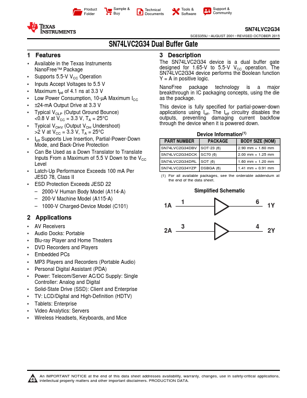
The SN74LVC2G34 device is a dual buffer gate designed for 1.65-V to 5.5-V VCC operation. The SN74LVC2G34 device performs the Boolean function Y = A in positive logic.
Nano Free package technology is a major breakthrough in IC...