• Part: SN74LVC8T245-Q1
  • Description: 8-Bit Dual-Supply Bus Transceiver
  • Manufacturer: Texas Instruments
  • Size: 0.96 MB
Download SN74LVC8T245-Q1 Datasheet PDF
Texas Instruments
SN74LVC8T245-Q1
SN74LVC8T245-Q1 is 8-Bit Dual-Supply Bus Transceiver manufactured by Texas Instruments.
Features - Control inputs VIH/VIL levels are referenced to VCCA voltage - VCC isolation feature - if either VCC input is at GND, all are in the high-impedance state - Fully configurable dual-rail design allows each port to operate over the full 1.65-V to 5.5-V powersupply range - Latch-up performance exceeds 100 m A per JESD 78, class II - ESD protection exceeds JESD 22 - 4000-V Human-Body Model (A114-A) - 100-V Machine Model (A115-A) - 1000-V Charged-Device Model (C101) 2 Applications - Personal electronic - Industrial - Enterprise - Tele 2 DIR 3 A1 22 OE 21 B1 To Seven Other Channels Logic Diagram (Positive Logic) 3 Description 
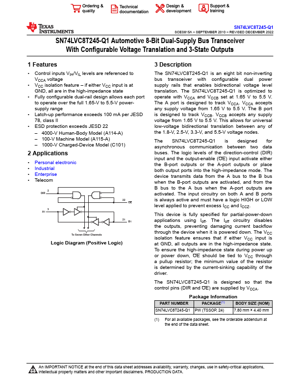
The SN74LVC8T245-Q1 is an eight bit non-inverting bus transceiver with configurable dual power supply rails that enables bidirectional voltage level translation. The SN74LVC8T245-Q1 is optimized to operate with VCCA and VCCB set at 1.65 V to 5.5 V. The A port is designed to track VCCA. VCCA accepts any supply voltage from 1.65 V to 5.5 V. The B port is designed to track VCCB. VCCB accepts any supply voltage from 1.65 V to 5.5 V. This allows for universal low-voltage bidirectional translation between any of the 1.8-V, 2.5-V, 3.3-V, and 5.5-V voltage nodes. The SN74LVC8T245-Q1 is designed for asynchronous munication between two data buses. The logic levels of the direction-control (DIR) input and the output-enable (OE) input activate either the B-port outputs or the A-port outputs or place both output ports into the high-impedance mode. The device transmits data from the A bus to the B bus when the B-port outputs are activated, and from the B bus to the A bus when the A-port outputs are activated. The input circuitry on both A and B ports is always active and must have a logic HIGH or LOW level applied to prevent excess ICC and ICCZ. This device is fully specified for partial-power-down applications using Ioff. The Ioff circuitry disables the outputs, preventing damaging current backflow through the device when it is powered down. The...