SN74SSTVF16857
description
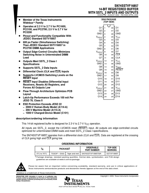
/ordering information
This 14-bit registered buffer is designed for 2.3-V to 2.7-V VCC operation. All inputs are SSTL_2, except the LVCMOS reset (RESET) input. All outputs are edge-controlled circuits optimized for unterminated DIMM loads and meet SSTL_2 Class I specifications.
The SN74SSTVF16857 operates from a differential clock (CLK and CLK). Data are registered at the crossing of CLK going high and CLK going low.
ORDERING INFORMATION
PACKAGE†
ORDERABLE PART NUMBER
TOP-SIDE MARKING
0°C to 70°C TSSOP
- DGG Tape and reel SN74SSTVF16857GR
SSTVF16857
† Package drawings, standard packing quantities, thermal data, symbolization, and PCB design guidelines are available at .ti./sc/package.
Please be aware that an important notice concerning availability, standard warranty, and use in critical applications of Texas Instruments semiconductor products and disclaimers thereto appears at the end of this data sheet.
Widebus is a trademark of Texas Instruments.
PRODUCTION...