SN75146
SN75146 is DUAL DIFFERENTIAL LINE RECEIVER manufactured by Texas Instruments.
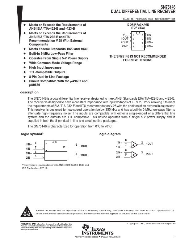
description
The SN75146 is a dual differential line receiver designed to meet ANSI Standards EIA / TIA-422-B and -423-B. The receiver is designed to have a constant impedance with input voltages of ± 3 V to ± 25 V allowing it to meet the requirements of EIA / TIA-232-E and ITU remendation V.28 with the addition of an external bias resistor. This receiver is designed for low-speed operation below 355 k Hz and has a built-in 5-MHz low-pass filter to attenuate high-frequency noise. The inputs are patible with either a single-ended or a differential line system and the outputs are TTL patible. This device operates from a single 5-V power supply and is supplied in both the 8-pin dual-in-line and small-outline packages.
The SN75146 is characterized for operation from 0°C to 70°C. logic symbol†
1IN + 1IN
- 2IN + 2IN
- 8 7 6 5
2 1OUT 3 2OUT logic diagram
1IN + 1IN
- 2IN + 2IN
- 8 7
6 5
2 1OUT 3 2OUT
† This symbol is in accordance with ANSI/IEEE Std 91-1984 and IEC Publication 617-12.
Please be aware that an important notice concerning availability, standard warranty, and use in critical applications of Texas Instruments semiconductor products and disclaimers thereto appears at the end of this data sheet.
PRODUCTION DATA information is current as of publication date. Products conform to specifications per the terms of Texas Instruments standard warranty. Production processing does not necessarily include testing of all parameters.
- POST OFFICE BOX 655303 DALLAS, TEXAS 75265
Copyright © 1995, Texas Instruments Incorporated 1
SN75146 DUAL DIFFERENTIAL LINE RECEIVER
SLLS015B
- FEBRUARY 1986
- REVISED MAY 1995 schematics of inputs and outputs
EQUIVALENT OF EACH INPUT
R1
Input
740 Ω NOM 7.4 kΩ NOM
740 Ω NOM
7.41 R1
TYPICAL OF ALL OUTPUTS VCC
50 Ω NOM
Output absolute maximum ratings over operating free-air temperature range (unless otherwise noted)†
Supply voltage range, VCC (see Note 1)
- -
- -
- - . . . ....