SNJ54AHC367J Overview
Description
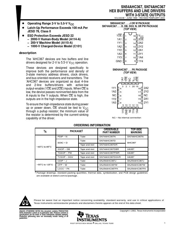
The ’AHC367 devices are hex buffers and line drivers designed for 2-V to 5.5-V VCC operation. These devices are designed specifically to improve both the performance and density of 3-state memory address drivers, clock drivers, and bus-oriented receivers and transmitters.