SNJ54HCT74J
SNJ54HCT74J is DUAL D-TYPE POSITIVE-EDGE-TRIGGERED FLIP-FLOPS manufactured by Texas Instruments.
Features
- Operating voltage range of 4.5 V to 5.5 V
- Outputs can drive up to 10 LSTTL loads
- Low power consumption, 40-μA max ICC
- Typical tpd = 17 ns
- ±4-m A output drive at 5 V
- Low input current of 1 μA max
- Inputs are TTL-voltage patible
2 Description
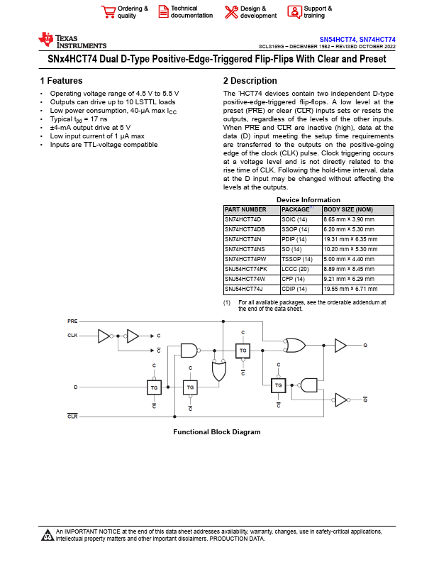
The ’HCT74 devices contain two independent D-type positive-edge-triggered flip-flops. A low level at the preset (PRE) or clear (CLR) inputs sets or resets the outputs, regardless of the levels of the other inputs. When PRE and CLR are inactive (high), data at the data (D) input meeting the setup time requirements are transferred to the outputs on the positive-going edge of the clock (CLK) pulse. Clock triggering occurs at a voltage level and is not directly related to the rise time of CLK. Following the hold-time interval, data at the D input may be changed without affecting the levels at the outputs.
PART NUMBER SN74HCT74D SN74HCT74DB SN74HCT74N SN74HCT74NS SN74HCT74PW SNJ54HCT74FK SNJ54HCT74W SNJ54HCT74J
Device Information
PACKAGE(1) BODY SIZE (NOM)
SOIC (14)
8.65 mm × 3.90 mm
SSOP (14)
6.20 mm × 5.30 mm
PDIP (14)
19.31 mm × 6.35 mm
SO (14)
10.20 mm × 5.30 mm
TSSOP (14) 5.00 mm × 4.40 mm
LCCC (20)
8.89 mm × 8.45 mm
CFP (14)
9.21 mm × 6.29 mm
CDIP (14)
19.55 mm × 6.71 mm
(1) For all available packages, see the orderable addendum at the end of the data sheet.
Functional Block Diagram
An IMPORTANT NOTICE at the end of this data sheet addresses availability, warranty, changes, use in safety-critical applications, intellectual property matters and other important disclaimers. PRODUCTION DATA.
SN54HCT74, SN74HCT74
SCLS169G
- DECEMBER 1982
- REVISED OCTOBER 2022
.ti.
Table of Contents
1 Features
1 2 Description
1 3 Revision History 2 4 Pin Configuration and Functions...