Datasheet4U Logo Datasheet4U.com

TLC277 - DUAL OPERATIONAL AMPLIFIERS

Download the TLC277 datasheet PDF. This datasheet also covers the TLC272 variant, as both devices belong to the same dual operational amplifiers family and are provided as variant models within a single manufacturer datasheet.

Description

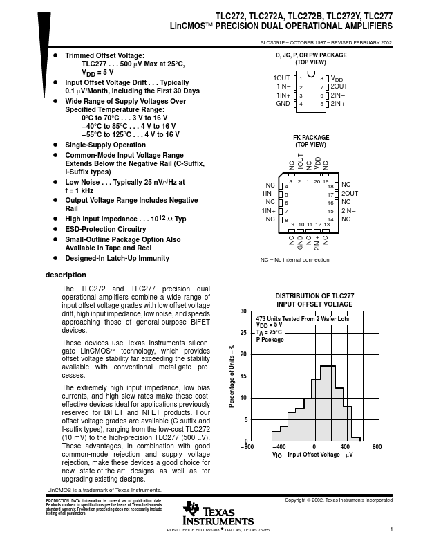
The TLC272 and TLC277 precision dual operational amplifiers combine a wide range of input offset voltage grades with low offset voltage drift, high input impedance, low noise, and speeds approaching those of general-purpose BiFET devices.

Features

  • associated with bipolar technology are available on LinCMOS operational amplifiers without the power penalties of bipolar technology. General.

📥 Download Datasheet

Note: The manufacturer provides a single datasheet file (TLC272-etcTI.pdf) that lists specifications for multiple related part numbers.

Full PDF Text Transcription

Click to expand full text
TLC272, TLC272A, TLC272B, TLC272Y, TLC277 LinCMOS PRECISION DUAL OPERATIONAL AMPLIFIERS D Trimmed Offset Voltage: TLC277 . . . 500 µV Max at 25°C, VDD = 5 V D Input Offset Voltage Drift . . . Typically 0.1 µV/Month, Including the First 30 Days D Wide Range of Supply Voltages Over Specified Temperature Range: 0°C to 70°C . . . 3 V to 16 V – 40°C to 85°C . . . 4 V to 16 V – 55°C to 125°C . . . 4 V to 16 V D Single-Supply Operation D Common-Mode Input Voltage Range Extends Below the Negative Rail (C-Suffix, I-Suffix types) D Low Noise . . . Typically 25 nV/√Hz at f = 1 kHz D Output Voltage Range Includes Negative Rail D High Input impedance . . .
Published: |