Texas Instruments TLC5510AI
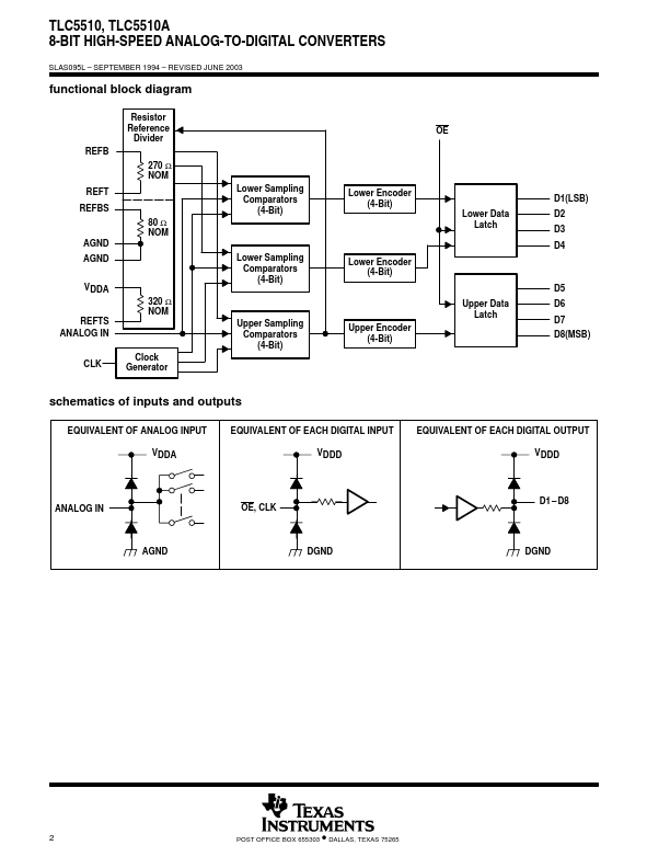
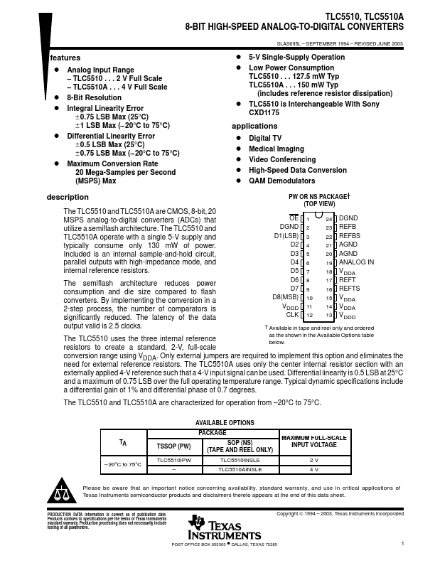
TLC5510 is Interchangeable With Sony CXD1175 applications D Digital TV D Medical Imaging D Video Conferencing D High-Speed Data Conversion D QAM Demodulators description PW OR NS PACKAGE† (TOP VIEW) The TLC5510 and TLC5510A are CMOS, 8-bit, 20 MSPS analog-to-digital converters (ADCs) that OE 1 24 DGND utilize a semiflash architecture. The TLC5510 and DGND 2 23 REFB TLC5510A operate with a single 5-V supply and D1(LSB) 3 22 REFBS typically consume only 130 mW of power. By implementing the conversion in a 2-step process, the number of comparators is significantly reduced.| Part No. | TLC5510AI |
|---|---|
| Datasheet | TLC5510AI Download |
| Manufacturer |  Texas Instruments |
| Description | 8-BIT HIGH-SPEED ANALOG-TO-DIGITAL CONVERTERS |
| Buy | Stock & Price |
DESCRIPTION
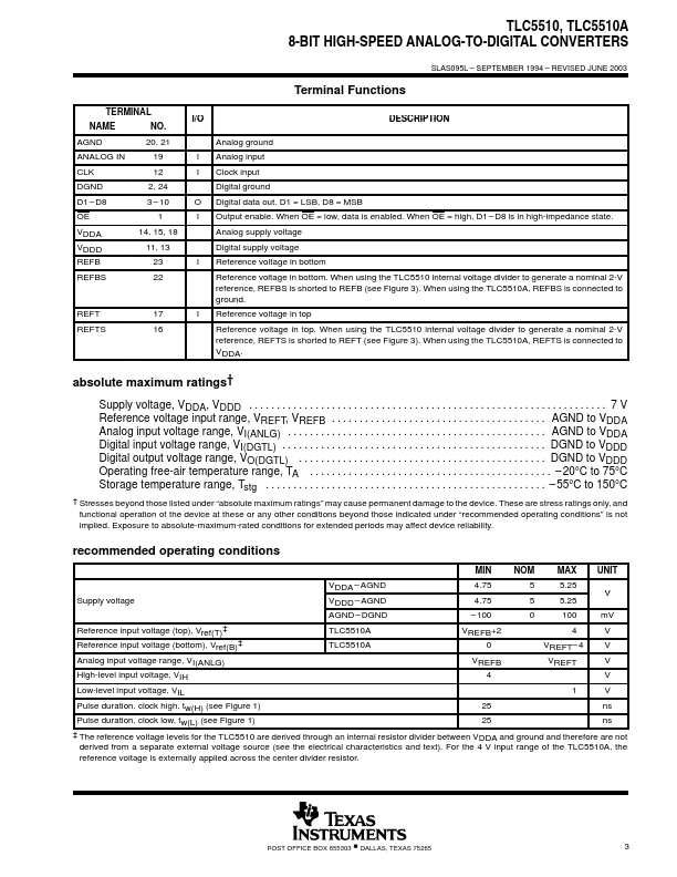
Analog ground I Analog input I Clock input Digital ground O Digital data out. D1 = LSB, D8 = MSB I Output enable. When OE = low, data is enabled. When OE = high, D1 – D8 is in high-impedance state. Analog supply voltage Digital supply voltage I Reference voltage in bottom Reference voltage in bottom. When using the TLC5510 internal voltage divider to generate a nominal 2-V reference, REFBS is shorted to REFB (see Figure 3). When using the TLC5510A, REFBS is connected to ground. I Reference voltage in top Reference voltage in top. When using the TLC5510 internal voltage divider to generate a no