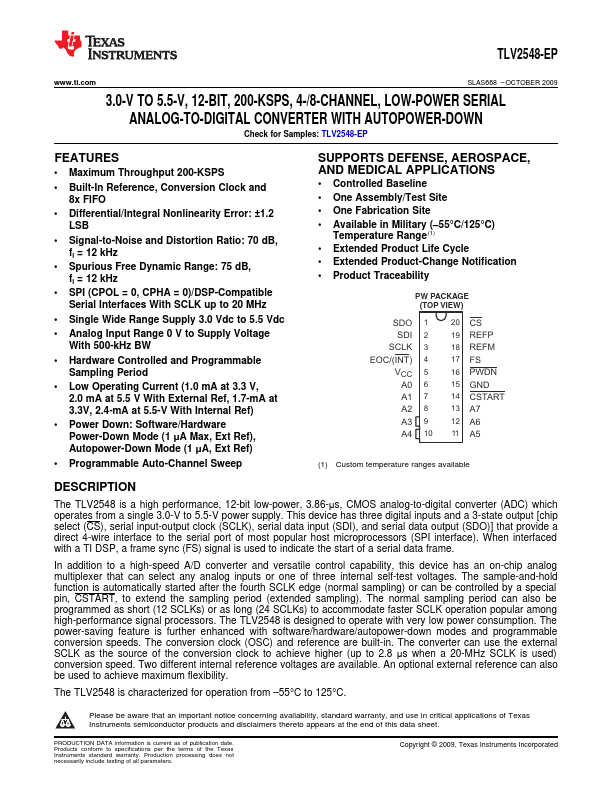
TLV2548-EP
FEATURES
- Maximum Throughput 200-KSPS
- Built-In Reference, Conversion Clock and 8x FIFO
- Differential/Integral Nonlinearity Error: ±1.2 LSB
- Signal-to-Noise and Distortion Ratio: 70 d B, fi = 12 k Hz
- Spurious Free Dynamic Range: 75 d B, fi = 12 k Hz
- SPI (CPOL = 0, CPHA = 0)/DSP-patible Serial Interfaces With SCLK up to 20 MHz
- Single Wide Range Supply 3.0 Vdc to 5.5 Vdc
- Analog Input Range 0 V to Supply Voltage With 500-k Hz BW
- Hardware Controlled and Programmable Sampling Period
- Low Operating Current (1.0 m A at 3.3 V, 2.0 m A at 5.5 V With External Ref, 1.7-m A at 3.3V, 2.4-m A at 5.5-V With Internal Ref)
- Power Down: Software/Hardware Power-Down Mode (1 μA Max, Ext Ref), Autopower-Down Mode (1 μA, Ext Ref)
- Programmable Auto-Channel Sweep
SUPPORTS DEFENSE, AEROSPACE, AND MEDICAL APPLICATIONS
- Controlled Baseline
- One Assembly/Test Site
- One Fabrication Site
- Available in Military (- 55°C/125°C)
Temperature Range(1)
- Extended Product Life Cycle
- Extended...