TMS27C128
TMS27C128 is Programmable ROM manufactured by Texas Instruments.
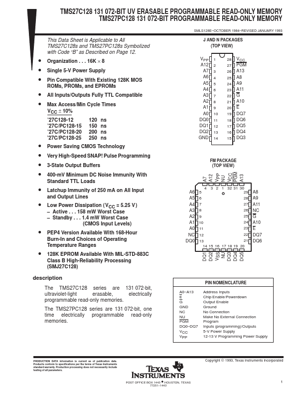
TMS27C128 131 072-BIT UV ERASABLE PROGRAMMABLE READ-ONLY MEMORY TMS27PC128 131 072-BIT PROGRAMMABLE READ-ONLY MEMORY
This Data Sheet is Applicable to All TMS27C128s and TMS27PC128s Symbolized with Code “B” as Described on Page 12.
- Organization . . . 16K × 8
- Single 5-V Power Supply
- Pin patible With Existing 128K MOS
ROMs, PROMs, and EPROMs
- All Inputs/Outputs Fully TTL patible
- Max Access/Min Cycle Times
VCC ± 10%
’27C128-12 ’27C/PC128-15 ’27C/PC128-20 ’27C/PC128-25
120 ns 150 ns 200 ns 250 ns
- Power Saving CMOS Technology
- Very High-Speed SNAP! Pulse Programming
- 3-State Output Buffers
- 400-m V Minimum DC Noise Immunity With
Standard TTL Loads
- Latchup Immunity of 250 m A on All Input and Output Lines
- Low Power Dissipation ( VCC = 5.25 V )
- Active . . . 158 m W Worst Case
- Standby . . . 1.4 m W Worst Case
(CMOS Input Levels)
- PEP4 Version Available With 168-Hour
Burn-In and Choices of Operating
Temperature Ranges
- 128K EPROM Available With MIL-STD-883C
Class B High-Reliability Processing
(SMJ27C128) description
The TMS27C128 series are 131 072-bit, ultraviolet-light erasable, electrically programmable read-only memories.
The TMS27PC128 series are 131 072-bit, one time electrically programmable read-only memories.
SMLS128E- OCTOBER 1984- REVISED JANUARY...