TPS22906
TPS22906 is Load Switch manufactured by Texas Instruments.
Features
2 Applications
- 1 Low-Input Voltage: 1.0 V to 3.6 V
- Ultra-Low ON-State Resistance
- r ON = 90 mΩ at VIN = 3.6 V
- r ON = 100 mΩ at VIN = 2.5 V
- r ON = 114 mΩ at VIN = 1.8 V
- r ON = 172 mΩ at VIN = 1.2 V
- 500-m A Maximum Continuous Switch Current
- Ultra-Low Quiescent Current: 82 n A at 1.8 V
- Ultra-Low Shutdown Current: 44 n A at 1.8 V
- Low Control Input Thresholds Enable Use of 1.2V/1.8-V/2.5-V/3.3-V Logic
- Controlled Slew Rate to Avoid Inrush Current: 220 μs tr
- ESD Performance Tested Per JESD 22
- 2000-V Human Body Model (A114-B, Class II)
- 1000-V Charged-Device Model (C101)
- Four-Terminal Wafer-Chip-Scale Package (WCSP)
- 0.9 mm × 0.9 mm, 0.5-mm Pitch, 0.5-mm Height
- Personal Digital Assistants (PDAs)
- Cellular Phones
- GPS Devices
- MP3 Players
- Digital Cameras
- Peripheral Ports
- Portable Instrumentation
- RF Modules
3 Description
TPS22906 device is an ultra-small, low ON-state resistance (r ON) load switch with controlled turn on. The device contains a P-channel MOSFET that operates over an input voltage range of 1.0 V to 3.6 V. The switch is controlled by an on/off input (ON), which is capable of interfacing directly with lowvoltage control signals. A 120-Ω on-chip load resistor is added for output quick discharge when the switch is turned off. TPS22906 is available in a space-saving 4-terminal WCSP with 0.5-mm pitch (YZV). The device is characterized for operation over the free-air temperature range of
- 40°C to 85°C.
Device Information(1)
PART NUMBER
PACKAGE
BODY SIZE (NOM)
DSBGA (4)
0.90 mm × 0.90 mm
(1) For all available packages, see the orderable addendum at the end of the data sheet.
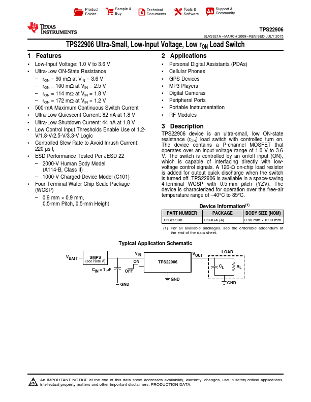
Typical Application Schematic
VBATT
SMPS
(see Note...