TPS22917L
Overview
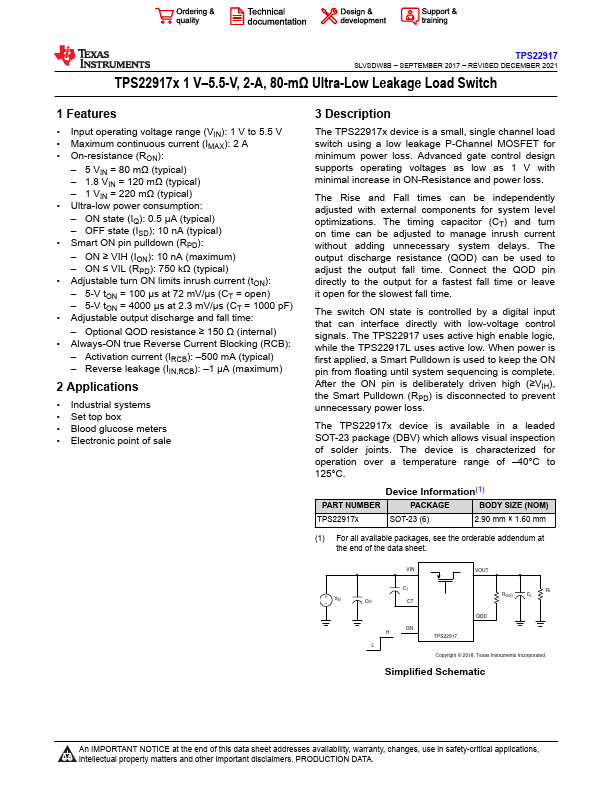
The TPS22917x device is a small, single channel load switch using a low leakage P-Channel MOSFET for minimum power loss. Advanced gate control design supports operating voltages as low as 1 V with minimal increase in ON-Resistance and power loss.
- Input operating voltage range (VIN): 1 V to 5.5 V
- Maximum continuous current (IMAX): 2 A
- On-resistance (RON): - 5 VIN = 80 mΩ (typical) - 1.8 VIN = 120 mΩ (typical) - 1 VIN = 220 mΩ (typical)
- Ultra-low power consumption: - ON state (IQ): 0.5 µA (typical) - OFF state (ISD): 10 nA (typical)
- Smart ON pin pulldown (RPD): - ON ≥ VIH (ION): 10 nA (maximum) - ON ≤ VIL (RPD): 750 kΩ (typical)
- Adjustable turn ON limits inrush current (tON): - 5-V tON = 100 μs at 72 mV/μs (CT = open) - 5-V tON = 4000 μs at 2.3 mV/μs (CT = 1000 pF)
- Adjustable output discharge and fall time: - Optional QOD resistance ≥ 150 Ω (internal)
- Always-ON true Reverse Current Blocking (RCB): - Activation current (IRCB): -500 mA (typical) - Reverse leakage (IIN,RCB): -1 µA (maximum)