Datasheet4U Logo Datasheet4U.com

TPS22925 - On-Resistance Load Switch

General Description

The TPS22925 product family consists of four devices: TPS22925B, TPS22925BN, TPS22925C, and TPS22925CN.

Each device is a 9-mΩ, singlechannel load switch with a controlled slew rate.

The devices contain an N–channel MOSFET that can operate over an input voltage range of 0.65 V to 3.6 V and can support a maximum continuous current of 3 A.

Overview

Product Folder Sample & Buy Technical Documents Tools & Software Support & Community TPS22925 SLVS840D – NOVEMBER 2015 – REVISED AUGUST 2016 TPS22925 3.

Key Features

  • 1 Input Voltage Range: 0.65 V to 3.6 V.
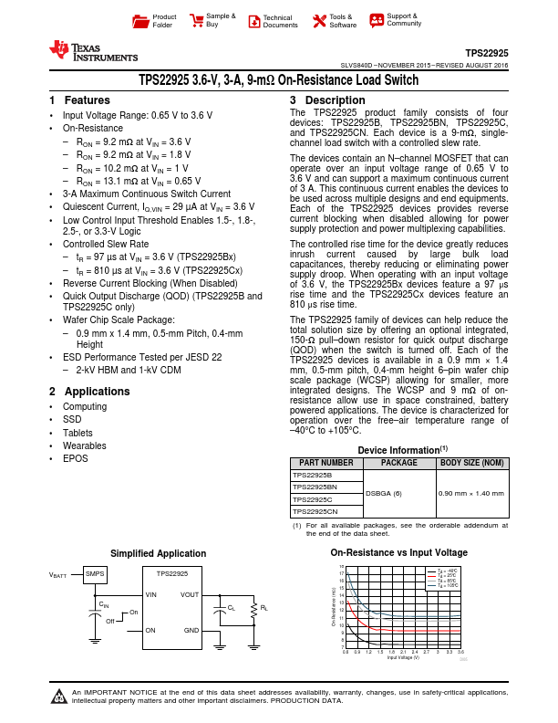
  • On-Resistance.
  • RON = 9.2 mΩ at VIN = 3.6 V.
  • RON = 9.2 mΩ at VIN = 1.8 V.
  • RON = 10.2 mΩ at VIN = 1 V.
  • RON = 13.1 mΩ at VIN = 0.65 V.
  • 3-A Maximum Continuous Switch Current.
  • Quiescent Current, IQ,VIN = 29 µA at VIN = 3.6 V.
  • Low Control Input Threshold Enables 1.5-, 1.8-, 2.5-, or 3.3-V Logic.
  • Controlled Slew Rate.
  • tR = 97 µs at VIN = 3.6 V (TPS22925Bx).