TPS51200-Q1
Overview
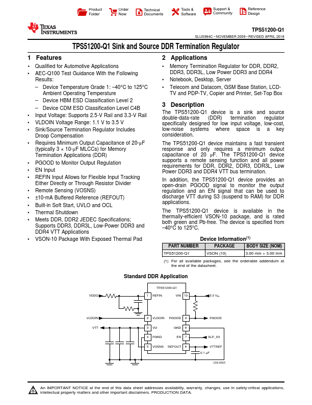
The TPS51200-Q1 device is a sink and source double-data-rate (DDR) termination regulator specifically designed for low input voltage, low-cost, low-noise systems where space is a key consideration. The TPS51200-Q1 device maintains a fast transient response and only requires a minimum output capacitance of 20 μF.
- 1 Qualified for Automotive Applications
- AEC-Q100 Test Guidance With the Following Results: - Device Temperature Grade 1: -40°C to 125°C Ambient Operating Temperature - Device HBM ESD Classification Level 2 - Device CDM ESD Classification Level C4B
- Input Voltage: Supports 2.5-V Rail and 3.3-V Rail
- VLDOIN Voltage Range: 1.1 V to 3.5 V
- Sink/Source Termination Regulator Includes Droop Compensation
- Requires Minimum Output Capacitance of 20-μF (typically 3 × 10-μF MLCCs) for Memory Termination Applications (DDR)
- PGOOD to Monitor Output Regulation
- EN Input
- REFIN Input Allows for Flexible Input Tracking Either Directly or Through Resistor Divider
- Remote Sensing (VOSNS)