TPS61096A
TPS61096A is 28-V Output Voltage Boost Converter manufactured by Texas Instruments.
Features
- 1 1 µA ultra-low IQ into VIN pin
- Operating Input Voltage from 1.8 V to 5.5 V
- Adjustable Output Voltage from 4.5 V to 28 V
- Selectable Inductor Peak Current:
- 0.25 A and 0.5 A
- Integrated Power Diode
- Integrated Level Shifters
- 70% Efficiency at 10 µA load
- 12-Pin 3-mm x 2-mm WSON Package
- Create a Custom Design Using the TPS61096A
With the WEBENCH® Power Designer
2 Applications
- Stylus
- Memory LCD Bias
- Sensor Power
- General Purpose Bias
- RF Mems Relay Power
3 Description
The TPS61096A is a high output voltage boost converter with ultra-low quiescent current. It is designed for products that require high efficiency at light load conditions powered by either two-cell alkaline, or one-cell Li-Ion or Li-polymer battery.
The TPS61096A integrates a 30-V power switch and a power diode. It can output up to 28 Volts. The TPS61096A uses a PFM peak current control scheme to obtain the highest efficiency over a wide range of input and output load conditions. It only consumes 1 µA quiescent current and can achieve up to 70% efficiency under 10-µA load condition.
The TPS61096A can also support selective inductor peak current. With 250-m A current limit, the TPS61096A can reduce inductor ripple so that it reduces external ponent size for light load applications. With 500 m A current limit, the TPS61096A can provide 30 m A output current for a conversion from 3.3 V to 18 V.
The TPS61096A integrates two-channel low-power level shifters to convert low level signals to output voltage level signals for specific applications. It only consumes 1-µA static current per channel and ensures very low static and dynamic power consumption across the entire output range.
The TPS61096A is available in a 12-pin 3.0-mm x 2.0-mm WSON Package.
Device Information(1)
PART NUMBER
PACKAGE
BODY SIZE (NOM)
WSON (12)
3 mm x 2 mm
(1) For all available packages, see the orderable addendum at the end of the data sheet.
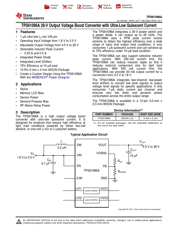
Typical Application Circuit
VIN 1.8 V to 5.5...