Texas Instruments TPS65140-Q1
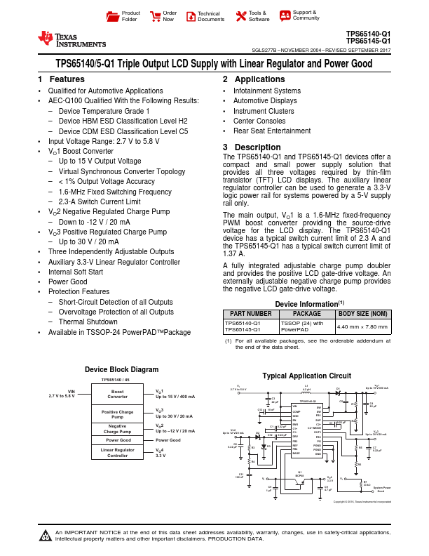
The TPS65140-Q1 and TPS65145-Q1 devices offer a compact and small power supply solution that provides all three voltages required by thin-film transistor (TFT) LCD displays. The auxiliary linear regulator controller can be used to generate a 3.3-V logic power rail for systems powered by a 5-V supply rail only. The main output, VO1 is a 1.6-MHz fixed-frequency PWM boost converter providing the source-drive voltage for the LCD display.| Part No. | TPS65140-Q1 |
|---|---|
| Datasheet | TPS65140-Q1 Download |
| Manufacturer |  Texas Instruments |
| Description | Triple Output LCD Supply |
| Buy | Stock & Price |
FEATURES
●1 Qualified for AutomotiveAPPLICATIONS
● AEC-Q100 Qualified With the Following Results: – Device Temperature Grade 1 – Device HBM ESD Classification Level H2 – Device CDM ESD Classification Level C5● Input Voltage Range: 2.7 V to 5.8 V
● VO1 Boost Converter – Up to 15 V Output Voltage – Virtual Synchronous Converter Topology – < 1% Output Voltage Accuracy – 1.6-MHz Fixed Switching Frequency – 2.3-A Switch Current Limit
● VO2 Negative Regulated Charge Pump – Down to -12 V / 20 mA
● VO3 Positive Regulated Charge Pump – Up to 30 V / 20 mA
● Three Independently Adjustable Outputs
● Auxiliary 3.3-V Linear Regulator Controller
● Internal Soft Start
● Power Good
● Protection
FEATURES
– Short-Circuit Detection of all Outputs – Overvoltage Protection of all Outputs – Thermal Shutdown● Available in TSSOP-24 PowerPAD™Package VIN 2.7 V to 5.8 V Device Block Diagram TPS65140 / 45 Boost Converter VO1 Up to 15 V / 400 mA Positive Charge Pump Negative Charge Pump Power Good Linear Regulat...