UCC21222-Q1
Overview
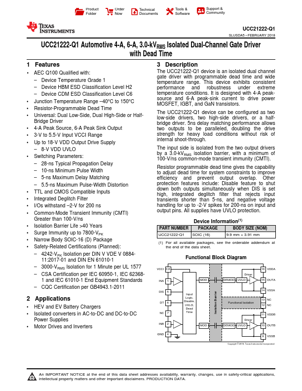
The UCC21222-Q1 device is an isolated dual channel gate driver with programmable dead time and wide temperature range. This device exhibits consistent performance and robustness under extreme temperature conditions.
- 1 AEC Q100 Qualified with: - Device Temperature Grade 1 - Device HBM ESD Classification Level H2 - Device CDM ESD Classification Level C6
- Junction Temperature Range -40°C to 150°C
- Resistor-Programmable Dead Time
- Universal: Dual Low-Side, Dual High-Side or Half- Bridge Driver
- 4-A Peak Source, 6-A Peak Sink Output
- 3-V to 5.5-V Input VCCI Range
- Up to 18-V VDD Output Drive Supply - 8-V VDD UVLO
- Switching Parameters: - 28-ns Typical Propagation Delay - 10-ns Minimum Pulse Width - 5-ns Maximum Delay Matching - 5.5-ns Maximum Pulse-Width Distortion
- TTL and CMOS Compatible Inputs
- Integrated Deglitch Filter