natlinear NP2N11MR
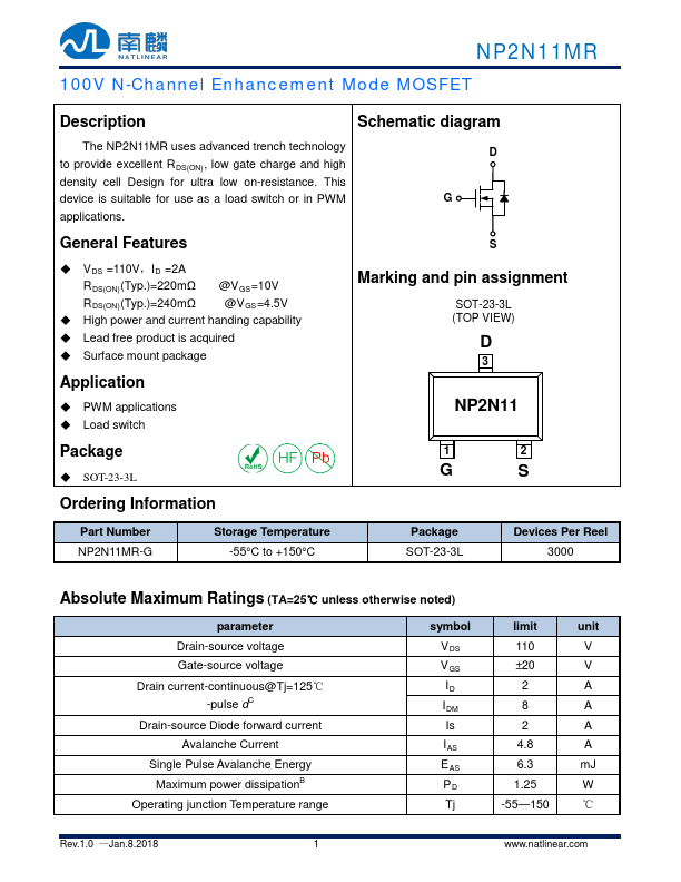
The NP2N11MR uses advanced trench technology to provide excellent RDS(ON), low gate charge and high density cell Design for ultra low on-resistance. This device is suitable for use as a load switch or in PWM applications. The value of RθJA is measured with the device mounted on 1in2 FR-4 board with 2oz.| Part No. | NP2N11MR |
|---|---|
| Datasheet | NP2N11MR Download |
| Manufacturer | natlinear |
| Description | 100V N-Channel Enhancement Mode MOSFET |
| Buy | Stock & Price |
DESCRIPTION
Schematic diagram D GGENERAL FEATURES
● VDS =110V,ID =2A RDS(ON)(Typ.)=220mΩ @VGS=10V RDS(ON)(Typ.)=240mΩ @VGS=4.5V● High power and current handing capability
● Lead free product is acquired
● Surface mount package Application
● PWM applications
● Load switch S Marking and pin assignment SOT-23-3L (TOP VIEW) D 3 NP2N11 Package
● SOT-23-3L 1 2 G S Ordering Information Part Number NP2N11MR-G Storage Temperature -55°C to +150°C Package SOT-23-3L Devices Per Reel 3000
ABSOLUTE MAXIMUM RATINGS
(TA=25℃ unless otherwise noted) parameter Drain-source voltage Gate-source voltage Drain current-continuous@Tj=125℃ -pulse dC Drain-source Diode forward current Avalanche Current Single Pulse Avalanche Energy Maximum power dissipationB Operating junction Temperature range symbol limit unit V DS 110 V V GS ±20 V ID 2 A IDM 8 A Is 2 A IAS 4.8 A E AS 6.3 mJ PD 1.25 W Tj -55—150 ℃ Rev.1.0 —Jan.8.2018 1 NP2N11MRELECTRICAL CHARACTERISTICS
(TA=25℃ unless otherwise noted) Parameter Symbol Condi...