Datasheet4U Logo Datasheet4U.com

74HC259-Q100 - 8-bit addressable latch

Datasheet Summary

Description

The 74HC259-Q100; 74HCT259-Q100 is an 8-bit addressable latch.

Features

  • Automotive product qualification in accordance with AEC-Q100 (Grade 1).
  • Specified from -40 °C to +85 °C and from -40 °C to +125 °C.
  • Wide supply voltage range from 2.0 V to 6.0 V.
  • Latch-up performance exceeds 100 mA per JESD 78 Class II Level B.
  • Complies with JEDEC standards:.
  • JESD8C (2.7 V to 3.6 V).
  • JESD7A (2.0 V to 6.0 V).
  • Combined demultiplexer and 8-bit latch.
  • Serial-to-parallel capability.
  • Output from.

📥 Download Datasheet

Datasheet preview – 74HC259-Q100

Datasheet Details

Part number 74HC259-Q100
Manufacturer nexperia
File Size 282.57 KB
Description 8-bit addressable latch
Datasheet download datasheet 74HC259-Q100 Datasheet
Additional preview pages of the 74HC259-Q100 datasheet.
Other Datasheets by nexperia

Full PDF Text Transcription

Click to expand full text
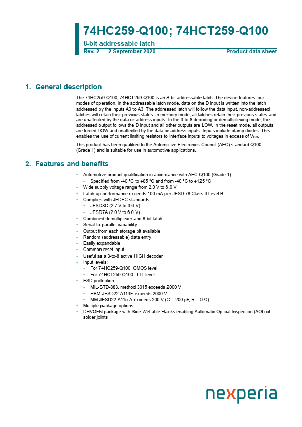
74HC259-Q100; 74HCT259-Q100 8-bit addressable latch Rev. 2 — 2 September 2020 Product data sheet 1. General description The 74HC259-Q100; 74HCT259-Q100 is an 8-bit addressable latch. The device features four modes of operation. In the addressable latch mode, data on the D input is written into the latch addressed by the inputs A0 to A3. The addressed latch will follow the data input, non-addressed latches will retain their previous states. In memory mode, all latches retain their previous states and are unaffected by the data or address inputs. In the 3-to-8 decoding or demultiplexing mode, the addressed output follows the D input and all other outputs are LOW. In the reset mode, all outputs are forced LOW and unaffected by the data or address inputs. Inputs include clamp diodes.
Published: |