Datasheet4U Logo Datasheet4U.com

74HC2G34-Q100 - Dual buffer gate

General Description

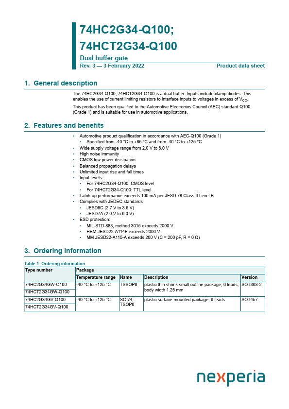
The 74HC2G34-Q100; 74HCT2G34-Q100 is a dual buffer.

Inputs include clamp diodes.

This enables the use of current limiting resistors to interface inputs to voltages in excess of VCC.

Key Features

  • Automotive product qualification in accordance with AEC-Q100 (Grade 1).
  • Specified from -40 °C to +85 °C and from -40 °C to +125 °C.
  • Wide supply voltage range from 2.0 V to 6.0 V.
  • High noise immunity.
  • CMOS low power dissipation.
  • Balanced propagation delays.
  • Unlimited input rise and fall times.
  • Input levels:.
  • For 74HC2G34-Q100: CMOS level.
  • For 74HCT2G34-Q100: TTL level.
  • Latch-up performance exceeds.

📥 Download Datasheet

Full PDF Text Transcription (Reference)

The following content is an automatically extracted verbatim text from the original manufacturer datasheet and is provided for reference purposes only.

View original datasheet text
74HC2G34-Q100; 74HCT2G34-Q100 Dual buffer gate Rev. 3 — 3 February 2022 Product data sheet 1. General description The 74HC2G34-Q100; 74HCT2G34-Q100 is a dual buffer. Inputs include clamp diodes. This enables the use of current limiting resistors to interface inputs to voltages in excess of VCC. This product has been qualified to the Automotive Electronics Council (AEC) standard Q100 (Grade 1) and is suitable for use in automotive applications. 2. Features and benefits • Automotive product qualification in accordance with AEC-Q100 (Grade 1) • Specified from -40 °C to +85 °C and from -40 °C to +125 °C • Wide supply voltage range from 2.0 V to 6.