Datasheet4U Logo Datasheet4U.com

74HC365 - Hex buffer/line driver

General Description

The 74HC365; 74HCT365 is a hex buffer/line driver with 3-state outputs controlled by the output enable inputs (OEn).

A HIGH on OEn causes the outputs to assume a high impedance OFF-state.

Inputs include clamp diodes.

Key Features

  • Wide supply voltage range from 2.0 V to 6.0 V.
  • CMOS low power dissipation.
  • High noise immunity.
  • Latch-up performance exceeds 100 mA per JESD 78 Class II Level B.
  • Complies with JEDEC standards:.
  • JESD8C (2.7 V to 3.6 V).
  • JESD7A (2.0 V to 6.0 V).
  • Non-inverting outputs.
  • Input levels:.
  • For 74HC365: CMOS level.
  • For 74HCT365: TTL level.
  • ESD protection:.
  • HBM JESD22-A114F exceed.

📥 Download Datasheet

Datasheet Details

Part number 74HC365
Manufacturer Nexperia
File Size 282.80 KB
Description Hex buffer/line driver
Datasheet download datasheet 74HC365 Datasheet

Full PDF Text Transcription (Reference)

The following content is an automatically extracted verbatim text from the original manufacturer datasheet and is provided for reference purposes only.

View original datasheet text
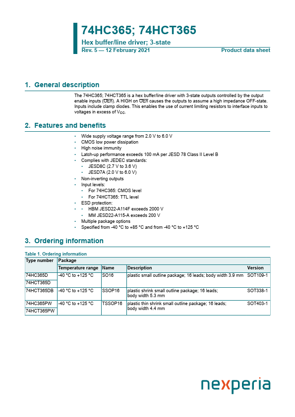
74HC365; 74HCT365 Hex buffer/line driver; 3-state Rev. 5 — 12 February 2021 Product data sheet 1. General description The 74HC365; 74HCT365 is a hex buffer/line driver with 3-state outputs controlled by the output enable inputs (OEn). A HIGH on OEn causes the outputs to assume a high impedance OFF-state. Inputs include clamp diodes. This enables the use of current limiting resistors to interface inputs to voltages in excess of VCC. 2. Features and benefits • Wide supply voltage range from 2.0 V to 6.0 V • CMOS low power dissipation • High noise immunity • Latch-up performance exceeds 100 mA per JESD 78 Class II Level B • Complies with JEDEC standards: • JESD8C (2.7 V to 3.6 V) • JESD7A (2.0 V to 6.