Datasheet4U Logo Datasheet4U.com

74HC4094-Q100 - 8-stage shift-and-store bus register

Datasheet Summary

Description

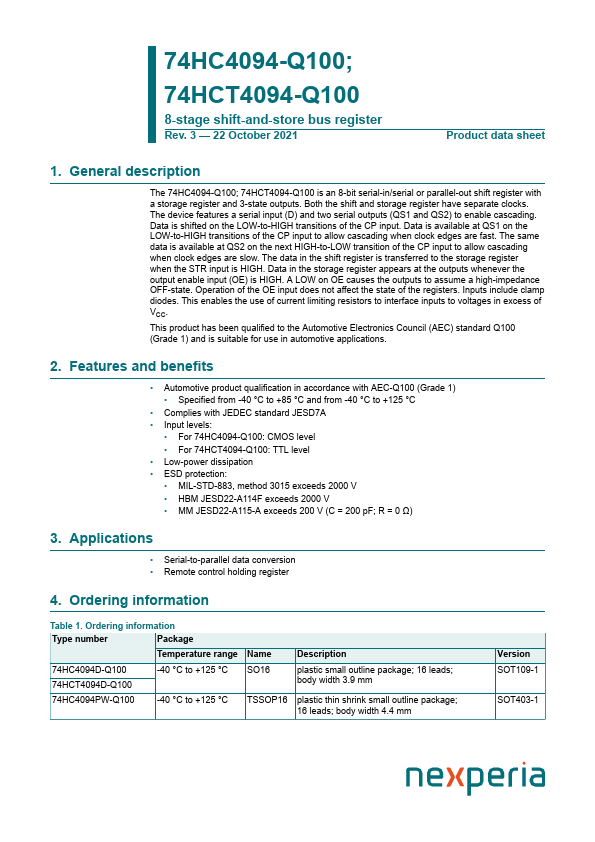
The 74HC4094-Q100; 74HCT4094-Q100 is an 8-bit serial-in/serial or parallel-out shift register with a storage register and 3-state outputs.

Both the shift and storage register have separate clocks.

Features

  • Automotive product qualification in accordance with AEC-Q100 (Grade 1).
  • Specified from -40 °C to +85 °C and from -40 °C to +125 °C.
  • Complies with JEDEC standard JESD7A.
  • Input levels:.
  • For 74HC4094-Q100: CMOS level.
  • For 74HCT4094-Q100: TTL level.
  • Low-power dissipation.
  • ESD protection:.
  • MIL-STD-883, method 3015 exceeds 2000 V.
  • HBM JESD22-A114F exceeds 2000 V.
  • MM JESD22-A115-A exceeds 200 V (C = 200.

📥 Download Datasheet

Datasheet preview – 74HC4094-Q100

Datasheet Details

Part number 74HC4094-Q100
Manufacturer nexperia
File Size 279.17 KB
Description 8-stage shift-and-store bus register
Datasheet download datasheet 74HC4094-Q100 Datasheet
Additional preview pages of the 74HC4094-Q100 datasheet.
Other Datasheets by nexperia

Full PDF Text Transcription

Click to expand full text
74HC4094-Q100; 74HCT4094-Q100 8-stage shift-and-store bus register Rev. 3 — 22 October 2021 Product data sheet 1. General description The 74HC4094-Q100; 74HCT4094-Q100 is an 8-bit serial-in/serial or parallel-out shift register with a storage register and 3-state outputs. Both the shift and storage register have separate clocks. The device features a serial input (D) and two serial outputs (QS1 and QS2) to enable cascading. Data is shifted on the LOW-to-HIGH transitions of the CP input. Data is available at QS1 on the LOW-to-HIGH transitions of the CP input to allow cascading when clock edges are fast. The same data is available at QS2 on the next HIGH-to-LOW transition of the CP input to allow cascading when clock edges are slow.
Published: |