Datasheet4U Logo Datasheet4U.com

74HC73D - Dual JK flip-flop

Download the 74HC73D datasheet PDF. This datasheet also covers the 74HC73 variant, as both devices belong to the same dual jk flip-flop family and are provided as variant models within a single manufacturer datasheet.

General Description

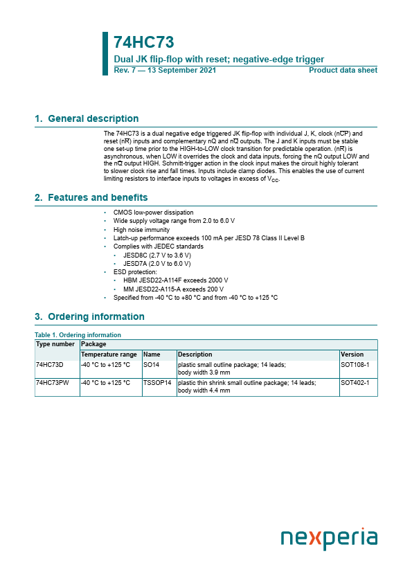
The 74HC73 is a dual negative edge triggered JK flip-flop with individual J, K, clock (nCP) and reset (nR) inputs and complementary nQ and nQ outputs.

The J and K inputs must be stable one set-up time prior to the HIGH-to-LOW clock transition for predictable operation.

Key Features

  • CMOS low-power dissipation.
  • Wide supply voltage range from 2.0 to 6.0 V.
  • High noise immunity.
  • Latch-up performance exceeds 100 mA per JESD 78 Class II Level B.
  • Complies with JEDEC standards.
  • JESD8C (2.7 V to 3.6 V).
  • JESD7A (2.0 V to 6.0 V).
  • ESD protection:.
  • HBM JESD22-A114F exceeds 2000 V.
  • MM JESD22-A115-A exceeds 200 V.
  • Specified from -40 °C to +80 °C and from -40 °C to +125 °C 3. Ordering infor.

📥 Download Datasheet

Note: The manufacturer provides a single datasheet file (74HC73-nexperia.pdf) that lists specifications for multiple related part numbers.

Full PDF Text Transcription (Reference)

The following content is an automatically extracted verbatim text from the original manufacturer datasheet and is provided for reference purposes only.

View original datasheet text
74HC73 Dual JK flip-flop with reset; negative-edge trigger Rev. 7 — 13 September 2021 Product data sheet 1. General description The 74HC73 is a dual negative edge triggered JK flip-flop with individual J, K, clock (nCP) and reset (nR) inputs and complementary nQ and nQ outputs. The J and K inputs must be stable one set-up time prior to the HIGH-to-LOW clock transition for predictable operation. (nR) is asynchronous, when LOW it overrides the clock and data inputs, forcing the nQ output LOW and the nQ output HIGH. Schmitt-trigger action in the clock input makes the circuit highly tolerant to slower clock rise and fall times. Inputs include clamp diodes. This enables the use of current limiting resistors to interface inputs to voltages in excess of VCC. 2.