Datasheet4U Logo Datasheet4U.com

74HCT3G34-Q100 - Triple buffer gate

This page provides the datasheet information for the 74HCT3G34-Q100, a member of the 74HC3G34-Q100 Triple buffer gate family.

Datasheet Summary

Description

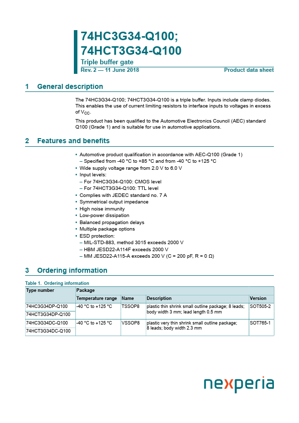
The 74HC3G34-Q100; 74HCT3G34-Q100 is a triple buffer.

Inputs include clamp diodes.

This enables the use of current limiting resistors to interface inputs to voltages in excess of VCC.

Features

  • Automotive product qualification in accordance with AEC-Q100 (Grade 1).
  • Specified from -40 °C to +85 °C and from -40 °C to +125 °C.
  • Wide supply voltage range from 2.0 V to 6.0 V.
  • Input levels:.
  • For 74HC3G34-Q100: CMOS level.
  • For 74HCT3G34-Q100: TTL level.
  • Complies with JEDEC standard no. 7 A.
  • Symmetrical output impedance.
  • High noise immunity.
  • Low-power dissipation.
  • Balanced propagation delays.

📥 Download Datasheet

Datasheet preview – 74HCT3G34-Q100

Datasheet Details

Part number 74HCT3G34-Q100
Manufacturer nexperia
File Size 191.11 KB
Description Triple buffer gate
Datasheet download datasheet 74HCT3G34-Q100 Datasheet
Additional preview pages of the 74HCT3G34-Q100 datasheet.
Other Datasheets by nexperia

Full PDF Text Transcription

Click to expand full text
74HC3G34-Q100; 74HCT3G34-Q100 Triple buffer gate Rev. 2 — 11 June 2018 Product data sheet 1 General description The 74HC3G34-Q100; 74HCT3G34-Q100 is a triple buffer. Inputs include clamp diodes. This enables the use of current limiting resistors to interface inputs to voltages in excess of VCC. This product has been qualified to the Automotive Electronics Council (AEC) standard Q100 (Grade 1) and is suitable for use in automotive applications. 2 Features and benefits • Automotive product qualification in accordance with AEC-Q100 (Grade 1) – Specified from -40 °C to +85 °C and from -40 °C to +125 °C • Wide supply voltage range from 2.0 V to 6.0 V • Input levels: – For 74HC3G34-Q100: CMOS level – For 74HCT3G34-Q100: TTL level • Complies with JEDEC standard no.
Published: |