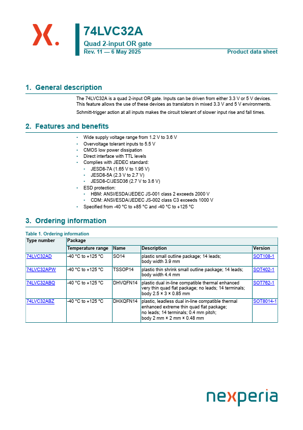
Datasheet4U Logo Datasheet4U.com

74LVC32AD - Quad 2-input OR gate

Download the 74LVC32AD datasheet PDF. This datasheet also covers the 74LVC32A variant, as both devices belong to the same quad 2-input or gate family and are provided as variant models within a single manufacturer datasheet.

General Description

The 74LVC32A is a quad 2-input OR gate.

Inputs can be driven from either 3.3 V or 5 V devices.

This feature allows the use of these devices as translators in mixed 3.3 V and 5 V environments.

Key Features

  • Wide supply voltage range from 1.2 V to 3.6 V.
  • Overvoltage tolerant inputs to 5.5 V.
  • CMOS low power dissipation.
  • Direct interface with TTL levels.
  • Complies with JEDEC standard:.
  • JESD8-7A (1.65 V to 1.95 V).
  • JESD8-5A (2.3 V to 2.7 V).
  • JESD8-C/JESD36 (2.7 V to 3.6 V).
  • ESD protection:.
  • HBM: ANSI/ESDA/JEDEC JS-001 class 2 exceeds 2000 V.
  • CDM: ANSI/ESDA/JEDEC JS-002 class C3 exceeds 1000 V.
  • Sp.

📥 Download Datasheet

Note: The manufacturer provides a single datasheet file (74LVC32A-nexperia.pdf) that lists specifications for multiple related part numbers.

Full PDF Text Transcription (Reference)

The following content is an automatically extracted verbatim text from the original manufacturer datasheet and is provided for reference purposes only.

View original datasheet text
74LVC32A Quad 2-input OR gate Rev. 11 — 6 May 2025 Product data sheet 1. General description The 74LVC32A is a quad 2-input OR gate. Inputs can be driven from either 3.3 V or 5 V devices. This feature allows the use of these devices as translators in mixed 3.3 V and 5 V environments. Schmitt-trigger action at all inputs makes the circuit tolerant of slower input rise and fall times. 2. Features and benefits • Wide supply voltage range from 1.2 V to 3.6 V • Overvoltage tolerant inputs to 5.5 V • CMOS low power dissipation • Direct interface with TTL levels • Complies with JEDEC standard: • JESD8-7A (1.65 V to 1.95 V) • JESD8-5A (2.3 V to 2.7 V) • JESD8-C/JESD36 (2.7 V to 3.