74LVC3G34 Description
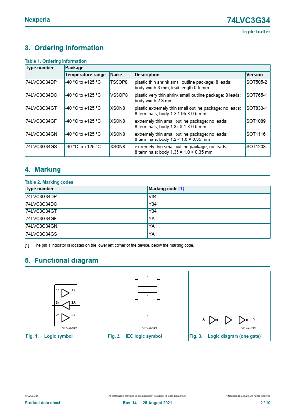
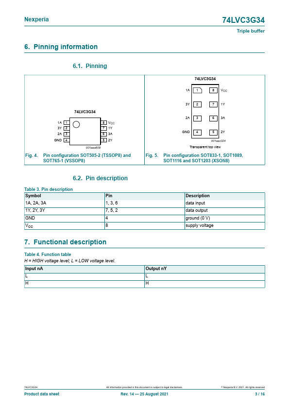
The 74LVC3G34 is a triple buffer. Inputs can be driven from either 3.3 V or 5 V devices.
74LVC3G34 Key Features
- Wide supply voltage range from 1.65 V to 5.5 V
- Overvoltage tolerant inputs to 5.5 V
- High noise immunity
- ±24 mA output drive (VCC = 3.0 V)
- CMOS low power consumption
- Latch-up performance exceeds 250 mA
- Direct interface with TTL levels
- plies with JEDEC standard
- JESD8-7 (1.65 V to 1.95 V)
- JESD8-5 (2.3 V to 2.7 V)
74LVC3G34 Applications
- Wide supply voltage range from 1.65 V to 5.5 V
- Overvoltage tolerant inputs to 5.5 V