Datasheet4U Logo Datasheet4U.com

74LVCH8T245-Q100 - 8-bit dual supply translating transceiver

Download the 74LVCH8T245-Q100 datasheet PDF. This datasheet also covers the 74LVC8T245-Q100 variant, as both devices belong to the same 8-bit dual supply translating transceiver family and are provided as variant models within a single manufacturer datasheet.

General Description

The 74LVC8T245-Q100; 74LVCH8T245-Q100 are 8-bit dual supply translating transceivers with 3-state outputs that enable bidirectional level translation.

Key Features

  • Automotive product qualification in accordance with AEC-Q100 (Grade 1).
  • Specified from -40 °C to +85 °C and from -40 °C to +125 °C.
  • Wide supply voltage range:.
  • VCC(A): 1.2 V to 5.5 V.
  • VCC(B): 1.2 V to 5.5 V.
  • High noise immunity.
  • Complies with JEDEC standards:.
  • JESD8-7 (1.2 V to 1.95 V).
  • JESD8-5 (1.8 V to 2.7 V).
  • JESD8C (2.7 V to 3.6 V).
  • JESD36 (4.5 V to 5.5 V).
  • ESD protection:.
  • M.

📥 Download Datasheet

Note: The manufacturer provides a single datasheet file (74LVC8T245-Q100-nexperia.pdf) that lists specifications for multiple related part numbers.

Full PDF Text Transcription (Reference)

The following content is an automatically extracted verbatim text from the original manufacturer datasheet and is provided for reference purposes only.

View original datasheet text
74LVC8T245-Q100; 74LVCH8T245-Q100 8-bit dual supply translating transceiver; 3-state Rev. 2 — 22 September 2020 Product data sheet 
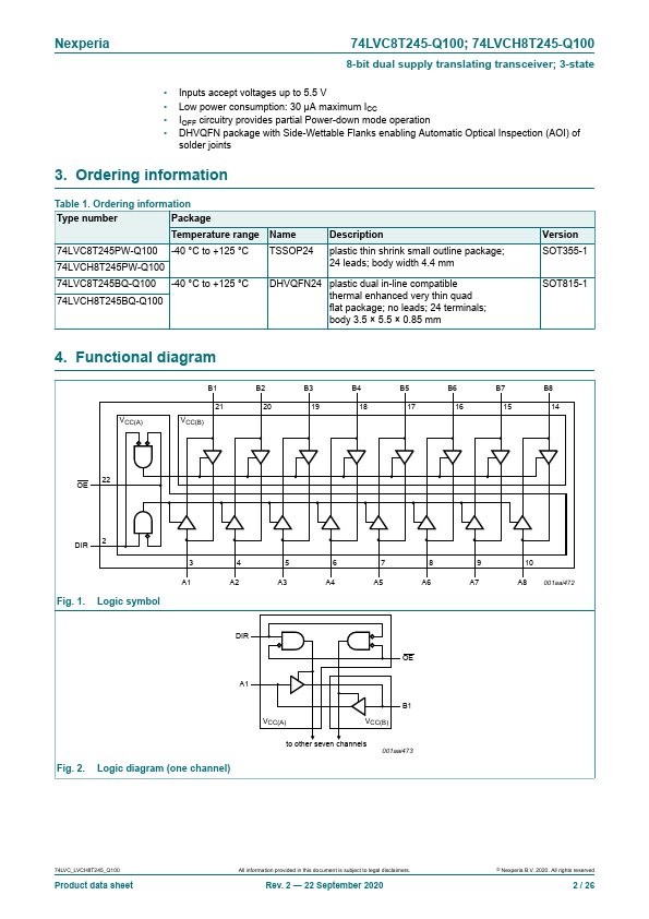
1. General description The 74LVC8T245-Q100; 74LVCH8T245-Q100 are 8-bit dual supply translating transceivers with 3-state outputs that enable bidirectional level translation. They feature two data input-output ports (pins An and Bn), a direction control input (DIR), an output enable input (OE) and dual supply pins (VCC(A) and VCC(B)). Both VCC(A) and VCC(B) can be supplied at any voltage between 1.2 V and 5.5 V. This flexibility makes the device suitable for translating between any of the low voltage nodes (1.2 V, 1.5 V, 1.8 V, 2.5 V, 3.3 V and 5.0 V). Pins An, OE and DIR are referenced to VCC(A) and pins Bn are referenced to VCC(B).