Nexperia BCM856DS
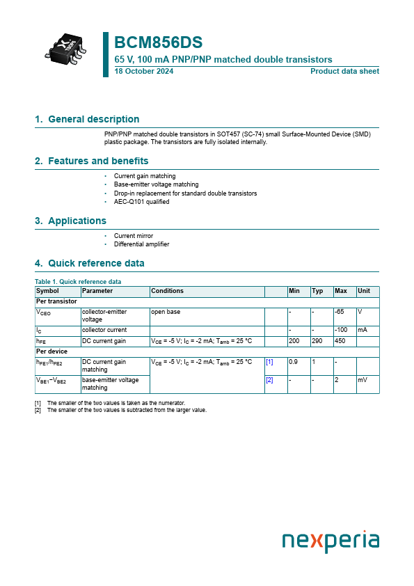
The transistors are fully isolated internally.| Part No. | BCM856DS |
|---|---|
| Datasheet | BCM856DS Download |
| Manufacturer |  Nexperia |
| Description | 100mA PNP/PNP matched double transistors |
| Buy | Stock & Price |
FEATURES AND BENEFITS
● Current gain matching● Base-emitter voltage matching
● Drop-in replacement for standard double transistors
● AEC-Q101 qualified 3.
APPLICATIONS
● Current mirror● Differential amplifier 4. Quick reference data Table 1. Quick reference data Symbol Parameter Conditions Per transistor VCEO collector-emitter voltage open base IC hFE Per device collector current DC current gain VCE = -5 V; IC = -2 mA; Tamb = 25 °C hFE1/hFE2 DC current gain matching VCE = -5 V; IC = -2 mA; Tamb = 25 °C [1] VBE1−VBE2 base-emitter voltage [2] matching [1] The smaller of the two values is taken as the numerator. [2] The smaller of the two values is subtracted from the larger value. Min Typ Max Unit - - -65 V - - -100 mA 200 290 450 0.9 1 - - - 2 mV Nexperia 5. Pinning information Table 2. Pinning information Pin Symbol
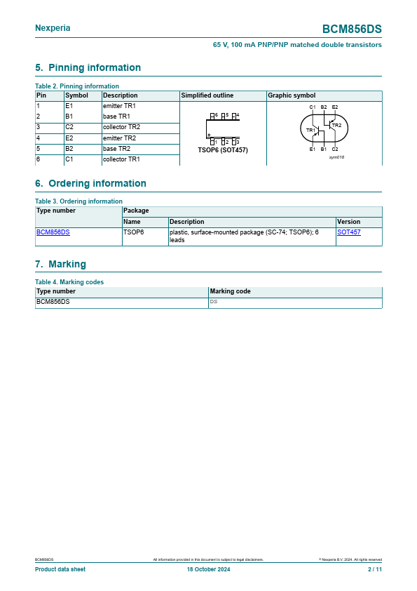
DESCRIPTION
1 E1 emitter TR1 2 B1 base TR1 3 C2 collector TR2 4 E2 emitter TR2 5 B2 base TR2 6 C1 collector TR1 6. Ordering information Table 3. Ordering information Type number Package Name BCM856DS TSOP6 7.